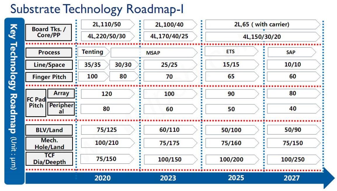
IC Substrate is the core interconnect carrier for advanced semiconductor chip packaging, serving as the critical bridge between semiconductor dies and printed circuit boards (PCBs). It is designed and manufactured in strict compliance with international industry standards including IPC-6016, IPC-9704 and JEDEC. Featuring ultra-high wiring density, micron-level fine line geometry, high-precision impedance control, and superior electrical and thermal management performance, IC substrates effectively match the high I/O density, high-speed signal transmission and high reliability requirements of advanced packaged chips. It is the core foundational component for high-end chip packaging in consumer electronics, automotive electronics, communication networks, AI computing, industrial control and other fields.
Core Product Series
1. System-in-Package (SiP) Substrate
SiP substrate is the core carrier for heterogeneous multi-chip integration, enabling the integration of semiconductor dies, passive components, sensing elements with different process nodes and functions into a single package structure. It provides IC designers with a system-level functional integration solution that delivers high integration, short R&D cycles and high flexibility, as an alternative to System-on-Chip (SoC).
- Full Structure Compatibility: Supports full range of structural designs including 2D planar Multi-Chip Module (MCM/MCP), 3D stacked packaging, Package-in-Package (PiP), and embedded component carrier boards
- Multi-Process Adaptation: Compatible with multiple interconnection methods including pure Wire Bonding (WB), Flip Chip (FC), and hybrid bonding, enabling diversified packaging combinations customized to customer requirements
- Key Advantages: Enables integration of heterogeneous chips from multiple sources, drastically reduces package size and thickness, shortens product R&D and time-to-market cycles, and lowers system-level integration costs
- Customization Service: Provides full-process design adaptation and flexible production according to customer product requirements, covering full-cycle needs from R&D prototyping to mass production
2. Plastic Ball Grid Array (PBGA) Substrate
PBGA substrate is the most widely used basic ball grid array packaging substrate for wire bonding processes. It is manufactured with glass fiber reinforced BT/FR-4 copper foil substrate, serving as an upgraded alternative to traditional lead frame packaging, and is perfectly suited for medium to high pin count chip packaging.
- Key Advantages: Supports higher I/O pin counts than traditional lead frames, with superior signal integrity and thermal performance, while delivering outstanding cost-effectiveness and excellent mass production stability
- Typical Applications: Packaging for mid-to-high end general-purpose chips including general-purpose Microcontroller Units (MCUs), consumer electronics main control chips, power management ICs, and industrial control chips
3. Flip Chip Chip Scale Package (FCCSP) Substrate
FCCSP substrate is a chip-scale packaging carrier adapted to flip chip processes. The die is directly interconnected with the substrate via metal bumps in a flip-chip configuration without wire bonding, with a package size close to the die size. It is the mainstream packaging solution for miniaturized, high-performance chips.
- Key Advantages: Extremely short interconnection path with low parasitic parameters and minimal signal transmission loss, delivering excellent high-frequency and high-speed performance; ultra-compact package size and thin profile, perfectly suited for extreme miniaturization designs; with the continuous maturity and cost reduction of wafer bumping processes, the cost-effectiveness of the solution continues to improve
- Typical Applications: Packaging for high pin count miniaturized chips in smartphones, wearable devices, IoT terminals, portable consumer electronics and other fields
4. Flip Chip Ball Grid Array (FCBGA) Substrate
FCBGA substrate is a high-density flip-chip packaging carrier for high-end high-performance chips, designed for large-size, ultra-high I/O pin count, high-speed LSI chips. It is a critical packaging supporting component for core chips in AI computing and high-end processors.
- Key Advantages: Supports tens of thousands of I/O pins, with extreme wiring density and signal integrity control capability, as well as excellent thermal management performance. It perfectly matches the high-speed computing and multi-channel signal transmission requirements of high-end chips, and has irreplaceable performance and cost advantages in ultra-high pin count chip packaging
- Typical Applications: High-performance computing fields including CPU/GPU, AI accelerator chips, high-end network processors, image processors, and automotive high-computing chips
MaxiPCB Core Manufacturing Capabilities
| Core Parameter |
Mass Production Capability |
Prototype Capability |
| Layer Count |
2 - 12 Layers |
Up to 20 Layers |
| Minimum Line Width/Spacing |
12μm/12μm |
8μm/8μm |
| Minimum Pad Size |
180μm |
120μm |
| Minimum Laser Microvia Diameter |
40μm |
30μm |
| Impedance Control Tolerance |
±5% |
±3% |
| Supported Package Types |
Full series: PBGA/FCCSP/SiP/FCBGA |
Customized advanced packaging substrates |
| Production Mode |
Large-scale mass production |
Rapid prototyping / small-batch trial production |
Design Support & Quality Assurance
Full-Process Design Service
We provide customers with end-to-end technical support for IC substrate design, covering the full process from packaging solution evaluation to Design for Manufacturability (DFM) optimization:
- Directly download MaxiPCB IC Substrate Design Rules document, fully aligned with mass production process requirements
- 1-on-1 technical support from our experienced packaging substrate engineering team to solve design difficulties and optimize solution manufacturability. Technical consultation email: sysdrn@163.com
Quality & Compliance Control
- The full production process strictly follows IPC-6016 Class 2/Class 3 and JEDEC international industry standards, with a fully closed-loop quality management system covering raw material incoming inspection, in-process SPC control, and finished product reliability testing
- All products fully comply with RoHS, REACH and other global environmental regulations, with stable batch consistency and high reliability, meeting the application requirements of automotive-grade, industrial-grade, consumer-grade and other different levels