1. Overview and Standard Definitions
1.1 Core Definition (IPC-2221)
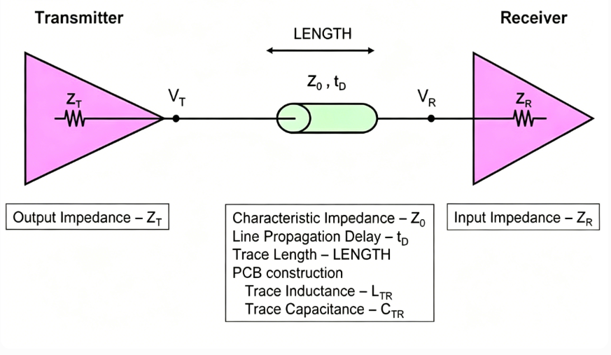
Characteristic Impedance (symbol: Z₀, unit: Ω) is the core IPC-standard parameter for high-speed and high-frequency PCB design. It refers to the steady-state ratio of signal voltage to signal current when a high-speed signal propagates along a PCB transmission line, determined by the distributed inductance (L) and distributed capacitance (C) of the transmission line. DC resistance (R) is negligible at high frequencies.
Industry Universal Standard Impedance Values:
- Single-ended lines: 50Ω (general high-speed/RF), 75Ω (video/cable TV), 60Ω (automotive Ethernet)
- Differential pairs: 100Ω (PCIe/DDR/USB4), 90Ω (USB 2.0/3.0), 85Ω (HDMI 2.1), 120Ω (CAN/LVDS)
1.2 Necessity of Impedance Control
Impedance matching is the foundation for solving Signal Integrity (SI) problems. Strict impedance control is mandatory when the physical length of the transmission line exceeds 1/6 of the electrical length corresponding to the signal rise time. Impedance mismatch will cause:
- Signal reflection, attenuation, and timing offset
- Increased crosstalk between lines
- Excessive EMI electromagnetic radiation
- Ultimately leading to signal distortion, system bit errors, or even functional failure
Mandatory Application Fields: 5G/6G communications, automotive ADAS, servers, medical devices, aerospace, RF antennas, and other high-reliability products.
2. Key Factors Affecting Characteristic Impedance (IPC-2221)
All parameters comply with IPC-2221 design specifications. The core correlations and mass production control requirements are as follows:
| Core Parameter |
Correlation with Impedance |
Industry Control Standard |
| Effective Dielectric Constant (εreff/Dkeff) |
Negative correlation (∝1/√εreff) |
Select low-loss, frequency-stable substrates for high-frequency designs; strictly control batch-to-batch Dk fluctuation ≤±0.05 |
| Dielectric Thickness Between Signal and Reference Layer (H) |
Positive correlation (primary adjustment parameter) |
Locked first during stack-up design; tolerance controlled within ±10% |
| Transmission Line Width (W) |
Negative correlation |
Strictly control etching undercut; implement targeted DFM line width compensation (compensation amount is positively correlated with copper thickness) |
| Total Copper Foil Thickness (T) |
Negative correlation |
Must include total thickness of base copper + electroplated copper; copper surface roughness effect must be considered for high-frequency designs |
| Differential Pair Coupling Spacing (S) |
Positive correlation (differential impedance only) |
Maintain consistent spacing throughout the entire trace length; tolerance controlled within ±0.05mm to ensure coupling stability |
| Solder Mask Thickness |
Negative correlation |
Must be included for surface layer traces; impedance difference between solder mask covered and exposed areas requires separate calculation |
| Copper Surface Roughness |
Negative correlation |
Roughness compensation required for designs above 10GHz; select RTF/VLP low-roughness copper foils |
Industry Misconception Correction: Precise impedance control can be achieved for 0.3oz to 10oz copper thickness through optimized line width compensation and process control. There is no technical upper limit at 2oz; 10oz heavy copper requires specialized heavy copper etching processes and lamination parameters.
3. Industry Standard Calculation Tools and Workflow
3.1 Mainstream Certified Calculation Tools
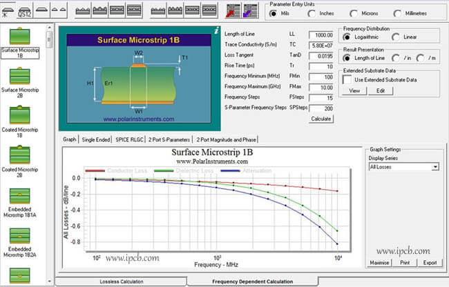
- Polar Si9000 Field Solver: Global industry benchmark, based on boundary element electromagnetic field model, supports accurate calculation of all mainstream transmission line structures
- Orbotech InPlan: Automated engineering system seamlessly integrated with Polar Si9000, enabling mass production-level batch impedance calculation, stack-up optimization, and automatic test coupon generation
- Substrate Manufacturer-Specific Tools: Dedicated calculators provided by Rogers, Isola, Panasonic and other manufacturers, optimized for their high-frequency low-loss materials
3.2 Standardized Calculation Workflow (Mandatory for Mass Production)
- Confirm target impedance values, tolerances, operating frequencies, and stack-up layer requirements with the PCB manufacturer
- Lock the manufacturer's actual measured process parameters (not substrate nominal values), including actual Dk, dielectric thickness tolerance, and etching compensation amount
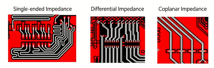
- Select the transmission line model matching the actual design (surface microstrip, embedded microstrip, stripline, coplanar waveguide)
- Calculate accurate line width/line spacing through Polar Si9000
- Apply mass production process compensation (line width compensation, copper thickness compensation, solder mask compensation)
- Freeze the design after completing cross-verification with the PCB manufacturer
4. IPC-Compliant Control and Test Specifications
4.1 Three-Tier Implementation Scheme
| Scheme Tier |
Standardized Process |
Applicable Scenarios |
Risk Level |
| Optimal Scheme |
Pre-calculation based on factory process parameters + full DFM verification before mass production |
High-speed/high-frequency, high-reliability products (automotive, medical, aerospace, servers) |
Extremely Low |
| Standard Scheme |
Clearly mark impedance requirements in design files, with professional compensation and verification completed by the manufacturer |
General industrial control, consumer electronics |
Low |
| Not Recommended |
Directly reuse past empirical values without pre-verification |
Only applicable to simple low-speed products with loose tolerance requirements |
High |
4.2 Impedance Test Specification (IPC-TM-650 2.5.5.7)
- Test Coupon Requirements: Impedance test coupons must be manufactured with the same stack-up, same process, and same materials as the production board, with a 1:1 structure matching the controlled traces on the board
- Standard Test Length: 150mm (6 inches), placed on the panel break-off edge (requires written customer confirmation of position)
- Test Method: Time Domain Reflectometry (TDR), strictly following IPC-TM-650 2.5.5.7 standard
- Acceptance Tolerances:
- General industrial grade: ±10%
- High-end consumer/industrial grade: ±5%
- RF/high-speed serial: ±3% (customized)
5. MaxiPCB Impedance Control Capabilities and Services
5.1 Core Technical Capabilities
| Core Parameter |
Mass Production Capability |
R&D Prototype Capability |
Industry Benchmark Level |
| Impedance Control Tolerance |
±5% (stable batch control) |
±3% (customized R&D) |
±5% |
| Supported Layer Count |
2~64 layers |
Up to 108 layers |
2~64 layers |
| Supported Operating Frequency |
Up to 40GHz |
Up to 110GHz |
Up to 40GHz |
| Supported Copper Thickness |
0.5oz~6oz |
0.3oz~10oz |
0.5oz~6oz |
| Test Capability |
100% full TDR testing, full data traceability |
High-frequency network analyzer impedance & insertion loss testing |
Sampling TDR testing |
5.2 Professional Value-Added Services
- Free stack-up design and impedance simulation services (based on Polar Si9000)
- Full-process DFM manufacturability audit for impedance designs
- Automated batch impedance engineering processing
- Complete test data traceability and official test reports
- 1-on-1 technical support from IPC-certified engineers

