Custom Printed Circuit Board (PCB) is a tailor-made circuit board designed and manufactured to match the specific electrical, mechanical, thermal and environmental requirements of a dedicated electronic product. Unlike general-purpose standard PCBs, custom PCBs enable full-dimensional customization of size, layer count, substrate material, structure, and electrical performance, making them the core carrier for specialized electronic devices and complex electronic systems.
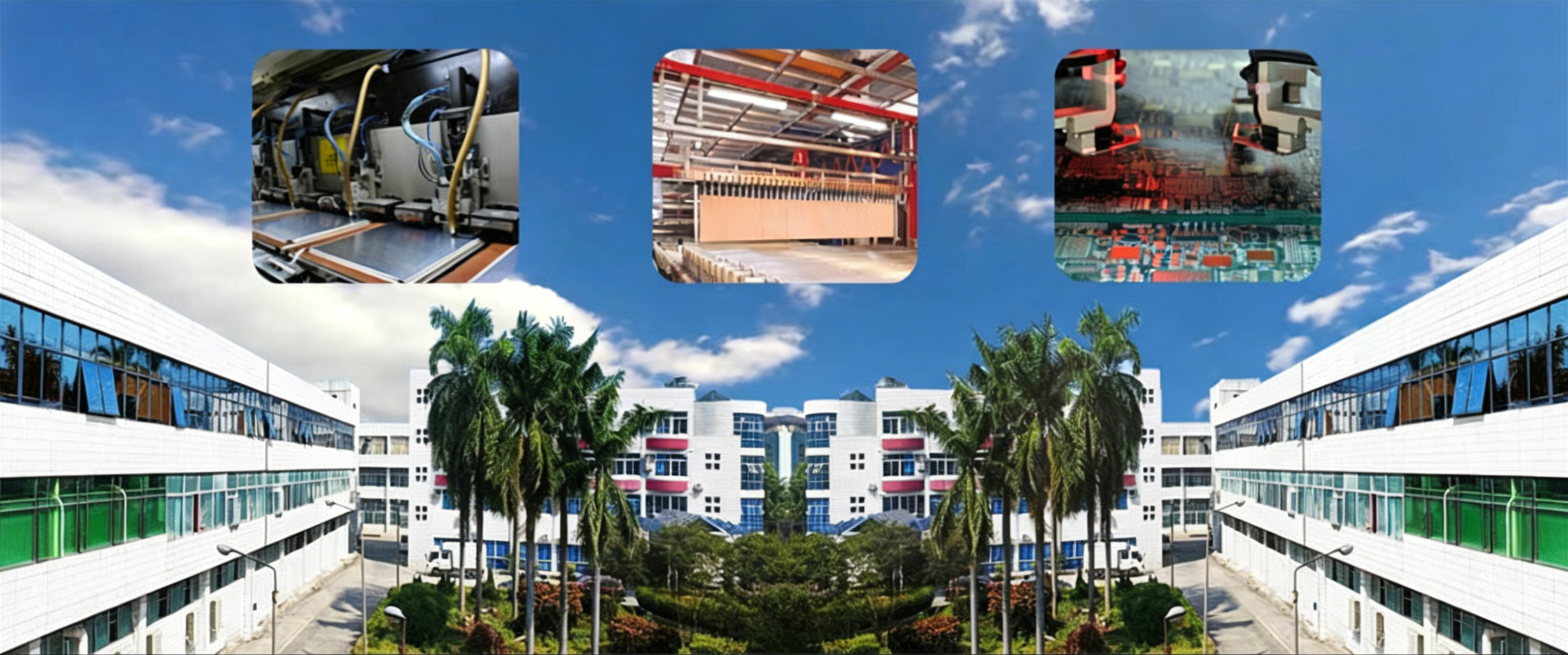
With over 10 years of in-depth industry experience, MaxiPCB is a leading global one-stop custom PCB manufacturing service provider. We strictly follow international industry standards including IPC-A-600, IPC-6012, and IPC-2221, providing global customers with full-chain customized services covering schematic design, DFM optimization, rapid prototyping, mass production, PCBA assembly, and full-process testing. Our solutions perfectly match the full-cycle needs of customers from R&D innovation to large-scale mass production.

Core Customization Service Matrix
1. Full-Process PCB Design & DFM Optimization Service
Our professional engineering team provides end-to-end design support to help customers turn product concepts into manufacturable, high-reliability PCB solutions:
- Schematic design, electrical rule check (ERC) and functional verification
- PCB stack-up design, impedance calculation and signal integrity (SI)/power integrity (PI) simulation
- Component layout, high-speed routing and electromagnetic compatibility (EMC) optimization
- Full-item Design for Manufacturability (DFM), Design for Assembly (DFA) and Design for Test (DFT) audits, to identify and resolve design risks in advance, reduce production scrap rate and shorten production cycle
2. Custom PCB Rapid Prototyping & Mass Production
We support full-category custom PCB manufacturing, with flexible production scheduling to meet both rapid prototyping for R&D and large-scale mass production needs. Our customizable product range covers:
- Standard rigid custom PCB (2~64 layers, mass production; up to 108 layers for R&D prototypes)
- High-frequency & high-speed custom PCB (Rogers, Arlon, Taconic, Nelco, Isola, PTFE, hydrocarbon and other special substrates, 4~32 layer hybrid lamination capability)
- HDI PCB, rigid-flex PCB, metal core PCB, ceramic PCB, IC substrate and IC test board
- Industry-specific custom PCB (custom keyboard PCB, custom LED PCB, automotive grade PCB, medical PCB, etc.)
3. Custom PCBA One-Stop Manufacturing Service
We set up a dedicated engineering project team for each custom PCBA project, and work closely with customers throughout the whole process:
- Pre-production NPI (New Product Introduction) review meeting, full-process DFM optimization for PCB manufacturing and assembly
- Full BOM component sourcing and quality verification, with global mainstream component supplier channels
- High-precision SMT (Surface Mount Technology) assembly, Through-Hole Technology (THT) soldering, and conformal coating services
- Full-process quality control, from incoming material inspection to finished product functional testing
4. Customized Testing & Compliance Certification Service
We provide customized testing solutions according to the project's industry and application scenarios, to ensure the product fully meets the required standards:
- Customized functional test fixture development and test procedure formulation
- Full testing capabilities including AOI (Automatic Optical Inspection), X-Ray inspection, ICT (In-Circuit Test), and FCT (Functional Circuit Test)
- Full compliance with RoHS, REACH, UL, IATF16949 and other global environmental and industry standards, with product conformity certification provided with shipment
- Support for customer-specific test procedures and standards, with full implementation and traceability throughout the testing process
Core Custom Manufacturing Capabilities
| Core Parameter |
Customizable Mass Production Range |
Extreme R&D Prototype Capability |
| Layer Count |
2~64 Layers |
Up to 108 Layers |
| Board Thickness |
0.15mm~8.0mm (Multilayer PCB); 0.10mm~8.0mm (Double-sided PCB) |
0.08mm~10.0mm |
| Minimum Finished Board Size |
0.5mm × 1.0mm |
Customized ultra-small size |
| Minimum Line Width/Line Spacing |
2/2mil (50/50μm) |
1/1mil (25/25μm) |
| Minimum Mechanical Drill Hole Diameter |
0.15mm |
0.1mm |
| Minimum Laser Blind Via Diameter |
50μm |
30μm |
| Maximum Aspect Ratio |
24:1 |
Up to 48:1 |
| Impedance Control Tolerance |
±5% |
±3% |
| High-Frequency Hybrid Lamination |
4~32 Layers |
Up to 40 Layers |
| Surface Finish |
HASL, ENIG, ENEPIG, OSP, Immersion Silver/Tin, Hard Gold, Customized Special Surface Finish |
Full range of special surface treatment customization |
Key Factors Affecting Custom PCB Cost
We work with customers to define the full scope of work based on custom specifications, and provide transparent project quotations to help achieve design requirements with optimal cost efficiency. The core factors affecting custom PCB cost include:
- Design Complexity: Layer count, line width/line spacing precision, via structure (blind/buried vias, stacked vias), impedance control requirements, and special process requirements
- Material Selection: Substrate type (standard FR-4, high-Tg FR-4, high-frequency low-loss substrate, metal core, ceramic, etc.), copper thickness, and brand of raw materials
- Production Requirements: Production quantity, delivery cycle, surface finish process, testing and certification requirements, and special assembly services
- Value-Added Services: Schematic design, layout optimization, DFM audit, component sourcing, PCBA assembly, and customized testing services
Professional Factory Customization vs. Traditional Homemade PCB
Traditional physical and chemical homemade PCB methods can no longer meet the precision, reliability and compliance requirements of modern electronic products. Our professional custom PCB manufacturing provides comprehensive advantages:
| Dimension |
Professional Custom PCB by MaxiPCB |
Traditional Homemade PCB (Physical/Chemical Method) |
| Fabrication Precision |
Micron-level precision control, stable batch consistency, support for ultra-fine lines and high-density routing |
Low precision, prone to broken lines, adhesion and short circuits, only suitable for simple circuits |
| Production Efficiency |
24-hour rapid prototyping for conventional boards, full-process automated production, no manual operation required |
Time-consuming and labor-intensive, requires repeated debugging and testing, long cycle and low efficiency |
| Reliability & Compliance |
Strictly follow IPC international standards, full-process quality control, 100% electrical testing before shipment, meet global environmental regulations |
Uncontrollable quality, no standardized testing, high scrap rate, toxic waste liquid is not environmentally friendly |
| Design Flexibility |
Support full-category complex structure PCB, high-frequency, HDI, rigid-flex and other customized designs |
Only support simple single/double-sided boards, cannot realize complex multilayer and special structure designs |
| Total Cost |
Optimized design reduces production and assembly costs, high cost performance for both prototyping and mass production |
High material and labor input for single board, serious scrap, no cost advantage |
Core Business Value of Custom PCB Solutions
With the trend of electronic product differentiation and customization, custom PCB has become the core driver to enhance product competitiveness:
- Differentiated Product Competition: Exclusive PCB design fully matches the unique functional requirements of the product, achieving performance that cannot be realized by standard PCBs, and building core technical barriers for products
- Full Lifecycle Cost Reduction: Optimized design eliminates redundant structure and materials, improves mass production yield, simplifies product assembly and maintenance processes, and reduces the total cost of ownership of the product
- Faster Time-to-Market: Our one-stop service from design to mass production shortens the R&D and verification cycle of new products, helping customers quickly respond to market demand and seize business opportunities
- Compliance & Reliability Guarantee: Customized design and manufacturing strictly follow industry standards, significantly improve the long-term operation stability of the product, reduce after-sales failure rate, and meet the compliance requirements of different industries
Who Needs Our Custom PCB Services?
- Innovative enterprises and start-up teams without in-house design and engineering capabilities, who need full-service support from product concept to finished product manufacturing
- Electronic enterprises with mature design solutions, who need professional, high-reliability PCB manufacturing and assembly services
- Industry customers with customized product requirements, including automotive electronics, medical devices, industrial control, communications, aerospace, consumer electronics and other fields
- Scientific research institutions and university laboratories, who need rapid prototyping and customized PCB solutions for R&D and innovation projects
Custom PCBA manufacturing
Frequently Asked Questions (FAQ)
-
What is a custom PCB?
A custom PCB is a printed circuit board designed and manufactured to meet the specific electrical, mechanical, thermal and environmental requirements of a dedicated project. Unlike general-purpose standard PCBs, custom PCBs can be fully tailored in terms of size, layer count, substrate material, structure and electrical performance to suit specialized electronic devices and complex systems.
-
What is the difference between custom PCB and standard PCB?
Standard PCBs are designed for general-purpose applications with fixed specifications, while custom PCBs are fully optimized for specific product designs, including layout, signal integrity, thermal management, mechanical structure and other dimensions. Custom PCBs are ideal for specialized electronic devices, high-complexity systems and products with differentiated functional requirements.
-
What PCB assembly services does MaxiPCB provide?
MaxiPCB provides complete end-to-end PCB Assembly (PCBA) services, including global component sourcing and quality verification, high-precision SMT surface mount assembly, through-hole (THT) soldering, conformal coating, and full functional testing for both prototype and mass production runs.
-
What files do I need to provide for custom PCB manufacturing?
To provide you with an accurate quotation and manufacturability assessment, you need to provide standard Gerber production files (including aperture table), PCB fabrication drawings, and BOM (Bill of Materials) for PCBA projects. We also support original design files from mainstream EDA software such as Altium Designer, KiCad and Cadence.
-
What is the typical lead time for custom PCB manufacturing and assembly?
Lead time depends on the design complexity, production quantity and process requirements. Conventional PCB prototypes can be completed in 24~72 hours, while mass production lead time is formulated according to order scale and factory scheduling. PCBA assembly lead time is matched with PCB production progress, and we provide expedited services for urgent projects. Submitting complete design files in advance can effectively shorten the delivery cycle.
-
Can you manufacture custom PCBs with complex designs?
Yes. We have full manufacturing capabilities for complex custom PCBs, including ultra-high-layer count boards, high-frequency & high-speed PCBs, high-order HDI PCBs, rigid-flex PCBs, metal core PCBs, ceramic PCBs and IC substrates. We also provide matching high-reliability PCBA assembly services for these advanced designs.
-
How do you ensure the quality of custom PCBs and assemblies?
MaxiPCB implements a full closed-loop quality control system throughout the design and manufacturing process. This includes pre-production DFM audit, in-process SPC statistical process control, AOI automatic optical inspection, X-Ray inspection, 100% electrical testing, and final functional testing. All production processes strictly follow IPC international standards to ensure stable and reliable product quality.

