Printed Circuit Board (PCB, formerly known as Printed Wiring Board, PWB), hailed as "the mother of electronic products", is the core foundational component of the global electronic information industry. Defined in strict accordance with IPC international industry standards, PCB is a bare board product that uses an insulating substrate as the carrier, forms a predetermined conductive pattern on the surface through a printing and etching process, and realizes electrical interconnection and signal transmission between electronic components. It should be clarified that a PCB with mounted integrated circuit components is a PCBA (Printed Circuit Board Assembly), which is an upstream and downstream link in the industrial chain and cannot be equated with a bare PCB.
As an indispensable core interconnection carrier for all electronic equipment, PCB provides mechanical support, electrical connection, signal transmission and circuit protection functions for components. It is widely used in the full spectrum of electronic manufacturing scenarios including consumer electronics, communication equipment, automotive electronics, industrial control, medical devices, and aerospace. With more than 10 years of in-depth experience in the PCB industry, MaxiPCB has full R&D, design and large-scale manufacturing capabilities for the full range of PCB products. We strictly follow international standards such as IPC-A-600 and IPC-6012, providing global customers with one-stop PCB solutions from schematic design, DFM audit, rapid prototyping to large-scale mass production.
Full-Range PCB Product System
In accordance with IPC international standards, combined with substrate characteristics, structural layers, electrical performance and application scenarios, we have built a full-range PCB product matrix that fully covers the diversified needs of customers:
1. Classification by Number of Conductive Layers
- Single-Sided PCB
With an insulating substrate with a thickness of 0.2mm~5.0mm as the carrier, only one side is clad with copper and a conductive pattern is formed by etching. Components and wires are placed on both sides of the board. It has the advantages of simple production process, low manufacturing cost and convenient assembly, and is suitable for electronic products with simple circuit structures such as radios, televisions and small household appliances, but not for high-density and complex circuit scenarios.
- Double-Sided PCB
Copper is clad on both sides of an insulating substrate with a thickness of 0.2mm~5.0mm, and conductive patterns are formed on both sides. Interlayer interconnection of the circuits on the front and back sides is realized through Plated Through Holes (PTH). Compared with single-sided boards, the wiring density is greatly improved, and the product volume is effectively reduced. It is suitable for medium-complexity general electronic equipment such as electronic computers and precision instruments, and is currently the most widely used basic PCB category.
- Multilayer PCB (MLB)
PCB products formed by alternately laminating 3 or more conductive pattern layers and insulating materials. The mainstream mass production in the industry is 4 to 64 layers, which can be divided into low-to-mid layer boards (4~8 layers), high-layer boards (10~20 layers), and ultra-high-layer boards (over 20 layers). Interlayer interconnection is realized through buried vias, blind vias and plated through holes. It has the core advantages of high wiring density, high integration, excellent signal integrity and strong anti-interference ability, and is the core carrier of high-end electronic equipment. At present, products are continuously upgraded towards high precision, high density, high reliability, thin profile and high-speed transmission.
2. Classification by Substrate Mechanical Properties
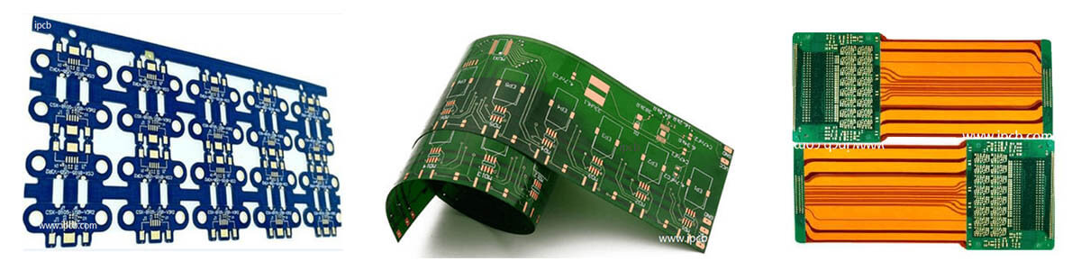
- Rigid PCB
With hard insulating substrates such as FR-4 epoxy glass cloth as the core, it has excellent mechanical strength and structural flatness, and can provide stable mechanical support for surface-mounted components. It is the most widely used PCB category in general electronic equipment.
- Flexible PCB (FPC)
With flexible insulating materials such as polyimide (PI) as the base material, it can be dynamically bent, curled and stretched, and can realize 3D space wiring according to the assembly requirements of the whole machine, effectively reducing the product volume. It is suitable for special scenarios requiring dynamic connection such as foldable screens, wearable devices, and vehicle-mounted displays.
- Rigid-Flex PCB
A composite structure PCB formed by integrating rigid substrates and flexible circuit layers through a lamination process. It combines the structural support of rigid boards and the 3D wiring capability of flexible boards, and is the preferred interconnection solution for high-reliability and miniaturized electronic systems. It is widely used in aerospace, medical equipment, high-end consumer electronics and other fields.
3. Classification by Electrical Performance & Application Scenarios
- General-Purpose PCB
With standard FR-4 substrate as the core, it is suitable for general electronic equipment with no special requirements for electrical performance, covering consumer electronics, small household appliances, general industrial control and other scenarios.
- High-Frequency & High-Speed PCB
Specially designed for microwave, millimeter-wave frequency bands and high-speed digital signal transmission scenarios, it adopts special substrates with low dielectric constant (Dk) and low dielectric loss tangent (Df) (such as PTFE, hydrocarbon resin, LCP, BT resin, etc.). It has excellent signal integrity and low transmission loss characteristics, and is the core carrier for 5G/6G communications, radar systems, high-speed servers, high-end routers and other products.
4. Special Process & Functional PCB
- Metal Core PCB (MCPCB)
It uses metal plates such as aluminum and iron plates to replace the traditional epoxy glass cloth substrate, and realizes electrical isolation between the conductive patterns on both sides of the metal plate and the metal part through an insulating layer. It has excellent heat dissipation performance, dimensional stability and electromagnetic shielding capability, and is suitable for scenarios with strict heat dissipation requirements such as high-power power supplies, LED lighting, and automotive electronics.
- Surface Mount PCB (SMB)
PCB products specially designed for Surface Mount Technology (SMT), with the characteristics of small aperture, fine line width and spacing, high precision and high substrate requirements. It is perfectly suitable for the assembly needs of high-density pin surface mount components, and is the mainstream supporting product for thin, light and miniaturized electronic equipment.
- Carbon Film PCB
A special PCB that forms a layer of carbon film through a printing process on the basis of the copper foil conductive pattern to realize the function of contacts, jumpers or resistors with preset resistance values. It has the characteristics of simple production process, low cost, good wear resistance and stable conductivity, which can greatly improve the wiring density of single-sided boards. It is suitable for consumer electronic products such as televisions, telephones, video recorders and electronic organs.
- Embedded Component PCB
High-end PCB products that embed passive components such as resistors, capacitors and magnetic components inside the PCB substrate. It can further improve wiring density and reduce product volume, and is suitable for high-density integration scenarios such as high-end portable electronics and communication modules.
Core Functional Value of PCB
As the core basic component of electronic equipment, PCB plays an irreplaceable core role in the whole machine system, and its core value is mainly reflected in the following dimensions:
- Core Carrier of Electrical Interconnection: Through the preset conductive pattern, it accurately realizes the circuit connection and signal relay transmission between various electronic components, ensuring the normal operation of the functions of the whole electronic system.
- Mechanical Support Base for Components: Provides stable and accurate mechanical installation and positioning for various electronic components, ensuring the orderly arrangement and structural stability of components in the whole machine.
- Safety Protection Barrier for Circuits: The solder mask on the surface can effectively avoid short circuit risks caused by solder overflow during the welding process, and the insulation properties of the substrate can realize reliable isolation of high and low voltage areas of the circuit, ensuring the safety of equipment and operators.
- Improved Production & Assembly Efficiency: Standardized PCB design and manufacturing greatly simplify the component welding and whole machine assembly processes, support full-process automated production and testing, effectively improve production efficiency, reduce manufacturing costs, and ensure product quality consistency.
- Simplified Equipment Maintenance & Upgrading: The highly integrated standardized PCB design makes equipment troubleshooting, component replacement and whole machine upgrading more convenient, without disassembling and reorganizing the whole machine, greatly reducing maintenance costs.
- High-Density Integration Capability: Through multi-layer structure design, micro blind and buried via technology and precision manufacturing technology, ultra-high-density circuit integration can be realized in a limited space, perfectly adapting to the development needs of miniaturization, thin profile and high performance of electronic equipment.
MaxiPCB Full-Process PCB Design & Manufacturing Services
We provide customers with professional technical support and manufacturing services covering the entire PCB design process, solving the full-cycle needs of customers from product solution to mass production:
- Schematic Design & Audit: Provide schematic design, Electrical Rules Check (ERC) and function verification services, optimize circuit design based on rich industry experience, and avoid principled design defects.
- PCB Stack-up & Impedance Planning: Provide professional stack-up design, impedance calculation and simulation services based on customers' signal transmission requirements, and provide dedicated stack-up optimization solutions for high-frequency and high-speed products to ensure signal integrity.
- Design for Manufacturability (DFM) Audit: Provide free full-process DFM audit services, conduct manufacturability, assemblability and testability checks on design documents, identify and optimize design risks in advance, reduce production scrap rate, and shorten production cycle.
- Layout & Routing and Signal Integrity Simulation: Provide professional PCB layout and routing services, and provide Signal Integrity (SI), Power Integrity (PI) and Electromagnetic Compatibility (EMC) simulation optimization for high-speed, high-frequency and high-power products to ensure that the product's electrical performance meets the standards.
- Standardized Production File Output & Verification: Provide generation and compliance inspection services for a full set of production files including standard Gerber production files, drill files, stencil files, and assembly drawings, to ensure that the files fully meet the mass production process requirements.
MaxiPCB Core Manufacturing Capabilities
| Core Parameter |
Mass Production Capability |
Prototype & R&D Capability |
| Layer Count |
2~64 Layers |
Up to 108 Layers |
| Minimum Line Width/Spacing |
2/2mil (50/50μm) |
1/1mil (25/25μm) |
| Minimum Mechanical Drill Hole Diameter |
0.15mm |
0.1mm |
| Minimum Laser Blind Via Diameter |
50μm |
30μm |
| Maximum Aspect Ratio |
24:1 |
Up to 48:1 |
| Impedance Control Tolerance |
±5% |
±3% |
| Maximum Processing Size |
2000mm × 650mm |
2300mm × 700mm |
| Surface Finish |
Full range of processes: HASL, ENIG, Immersion Silver, Immersion Tin, OSP, Hard Gold, Electroplated Gold |
Customized special surface finish |
| Substrate Compatibility |
Full range of substrates: FR-4, High-Tg FR-4, Low-Loss Substrate, PTFE, Metal Substrate, PI, etc. |
Customized special substrates |
Quality Assurance & Compliance Certification
- The full production process strictly follows IPC-A-600 and IPC-6012 Class 2/Class 3 international standards, and we have established a fully closed-loop quality management system covering raw material incoming inspection, in-process SPC statistical process control, finished product full electrical testing and reliability verification.
- We have passed ISO9001 Quality Management System Certification, UL Safety Certification, and IATF16949 Automotive Industry Quality Management System Certification. All products fully comply with global environmental regulations such as RoHS (Restriction of Hazardous Substances) and REACH.
- With a senior technical team with more than 10 years of industry experience and standardized intelligent production lines, the mass production yield of products is stably above 99.2%, the on-time delivery rate exceeds 98%, and products are exported to more than 30 countries and regions around the world.
