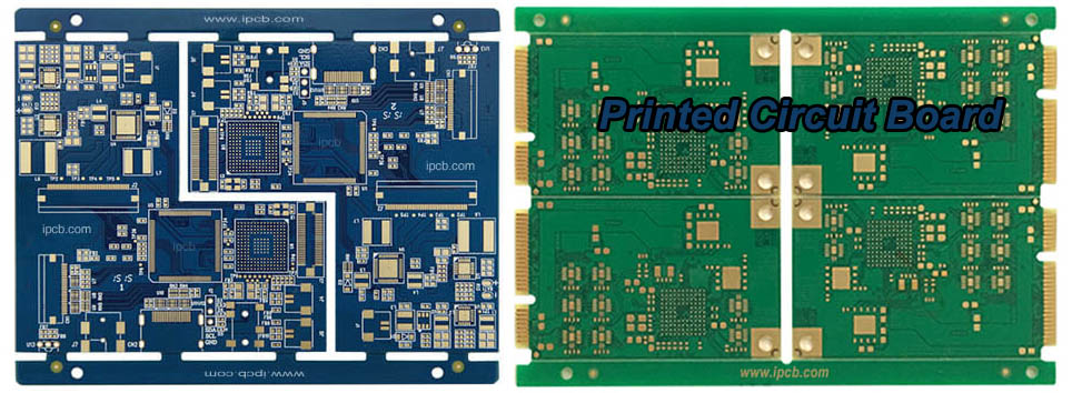
Printed Circuit Board (PCB, formerly known as Printed Wiring Board, PWB) is the core foundational component of the global electronic information industry, defined in strict accordance with IPC international standards. It is an interconnect carrier that forms predetermined conductive patterns on an insulating substrate through printing, etching and other processes, to realize electrical connection and signal transmission between electronic components.
With a development history of more than 100 years, PCB has evolved from an alternative wiring solution in the early 20th century to an absolutely dominant core component in the modern electronics industry. In 1925, American inventor Charles Ducas pioneered the technology of printing circuit patterns on insulating substrates and forming conductive wiring through electroplating, laying the foundation for modern PCB manufacturing. The core value of PCB lies in greatly reducing wiring and assembly errors in electronic product manufacturing, significantly improving the automation level and production efficiency of electronic products, and providing a reliable, miniaturized and high-integration interconnect solution for all kinds of electronic equipment.
Standard PCB Core Structure & Functional Composition
In line with IPC-2221 design standards, a standard PCB consists of the following core functional structures, each with strict industry specifications for design and manufacturing:
- Conductive Pattern
The core functional layer for electrical interconnection, including signal traces, power planes and ground planes. It is formed by precision etching of copper foil, realizing signal transmission between components and power distribution of the whole system. Large-area copper planes are usually designed as ground and power layers to optimize power integrity and electromagnetic shielding performance.
- Dielectric Substrate
The insulating core material of PCB, used to maintain reliable electrical isolation between conductive traces and different circuit layers, also known as the base material. Common materials include FR-4 epoxy glass cloth, high-Tg resin, PTFE high-frequency substrate, polyimide (PI) flexible substrate, etc. It is divided into rigid substrate, flexible substrate and rigid-flex composite substrate according to mechanical properties, to meet the needs of different application scenarios.
- Via Structure
The core structure to realize interlayer circuit interconnection, divided into three categories according to IPC standards:
- Plated Through Hole (PTH): Metalized through holes for electrical connection between different circuit layers
- Non-Plated Through Hole (NPTH): Non-metalized holes for component positioning, mounting hole fixation and mechanical installation
- Blind/Buried Vias: Microvias for interconnection between adjacent layers, without penetrating the whole board, for high-density HDI PCB designs
- Solder Mask
An insulating protective layer printed on the surface of the PCB, covering the non-soldering areas of the copper traces. It prevents short circuits caused by solder overflow during the welding process, protects the circuit from oxidation and corrosion, and improves the long-term reliability of the board. Conventional solder mask is green, and we also support customized colors including red, blue, black, white and matte options.
- Silkscreen Legend
A non-electrical functional layer printed on the surface of the PCB, used to mark component reference designators, polarity indicators, mounting frames, dimension labels and other text and graphic information. It provides clear guidance for component assembly, product debugging, later maintenance and repair.
MaxiPCB Core Manufacturing Capabilities
The core technical watershed of the PCB manufacturing industry lies in precision electroplating and etching process control, which directly determines the upper limit of product precision, yield and reliability. With more than 10 years of in-depth technology accumulation, MaxiPCB has mastered the industry-leading precision electroplating and etching core technology, with a full set of imported high-precision production equipment and sufficient raw material inventory, providing stable, high-reliability PCB manufacturing services for global customers.
| Core Manufacturing Parameter |
Mass Production Capability |
R&D Prototype Capability |
| Maximum Layer Count |
2~64 Layers |
Up to 108 Layers |
| Minimum Line Width/Line Spacing (Standard FR-4) |
3/3mil (75/75μm) |
2/2mil (50/50μm) |
| Minimum Line Width/Line Spacing (HDI PCB) |
2/2mil (50/50μm) |
1.5/1.5mil (35/35μm) |
| Minimum Line Width/Line Spacing (IC Substrate) |
30/30μm |
8/8μm |
| Minimum Mechanical Drill Hole Diameter |
0.15mm |
0.1mm |
| Minimum Laser Microvia Diameter |
50μm |
30μm |
| Maximum Aspect Ratio |
24:1 |
Up to 48:1 |
| Impedance Control Tolerance |
±5% |
±3% |
| Supported Substrates |
FR-4, High-Tg FR-4, Low-Loss Material, PTFE High-Frequency Substrate, Metal Core, Ceramic, PI, etc. |
Full Range of Custom Special Substrates |
| Surface Finish |
HASL, ENIG, ENEPIG, OSP, Immersion Silver/Tin, Hard Gold, Customized Special Process |
Full Range of Surface Finish Customization |
We have in-depth technical accumulation in microwave high-frequency PCB, high-order HDI PCB, IC substrate, rigid-flex PCB and other high-end product fields, with mature mass production processes and stable batch yield.
One-Stop PCBA Manufacturing & Compliance Testing Service
Printed Circuit Board Assembly (PCBA) is the finished product formed by mounting and welding electronic components on the bare PCB. We provide end-to-end one-stop PCBA manufacturing services, with strict compliance with global electronic manufacturing industry standards:
Full-Process Assembly Capabilities
- Global component sourcing and incoming quality verification, with authorized channels for mainstream component brands
- High-precision SMT (Surface Mount Technology) assembly, THT (Through-Hole Technology) soldering, and selective soldering services
- Full structural assembly services, including radiator installation, CPU base and backplate fixation, insulating Mylar sheet assembly, fastener installation and other auxiliary parts assembly
- Conformal coating, potting and other protective process services for harsh environment application scenarios
Standardized Testing & Quality Control System
- Full visual and electrical testing: AOI (Automatic Optical Inspection), X-Ray inspection for BGA/QFN components, ICT (In-Circuit Test) and FCT (Functional Circuit Test)
- ESD (Electrostatic Discharge) Protection: The whole production process strictly follows the ANSI/ESD S20.20 international standard. All assembly fixtures must pass ESD performance verification before being put into the production line, to prevent electrostatic damage to electrostatic sensitive devices such as ICs
- Mechanical Stress Control: All assembly fixtures and products are strictly tested in accordance with the IPC/JEDEC-9704A standard, to avoid mechanical stress damage to PCB and components during the assembly process
- Full-process polarity management: Strict anti-error control for polar components such as batteries, capacitors and diodes, to ensure 100% correct installation of polar components
Full-Process PCB Design Technical Support
We provide professional technical support covering the whole PCB design cycle, helping customers achieve high-reliability, high-manufacturability PCB design solutions:
- Pre-Design Planning: Schematic diagram review and electrical rule check (ERC), component package library verification, board outline and mechanical structure adaptation planning, PCB stack-up and impedance scheme design
- Layout & Routing Optimization: Component layout optimization, high-speed signal routing design, impedance matching control, and SI (Signal Integrity)/PI (Power Integrity)/EMC (Electromagnetic Compatibility) simulation services
- Full-Item DFM Audit: Free Design for Manufacturability (DFM), Design for Assembly (DFA) and Design for Test (DFT) audits, to identify and resolve design risks in advance, optimize mass production yield and reduce manufacturing costs
- Production File Standardization: Compliance check and standardized output of full set of production files, including Gerber files, drill files, stencil files, assembly drawings and fabrication specifications, to ensure the files fully match the mass production process requirements
Quality Assurance & Compliance Certification
- All products are manufactured in strict accordance with IPC-A-600, IPC-6012 Class 2/Class 3 international acceptance standards, with a fully closed-loop quality management system covering raw material incoming inspection, in-process SPC statistical process control, and finished product 100% electrical testing
- We have passed ISO9001 Quality Management System Certification, UL Safety Certification, IATF16949 Automotive Industry Quality Management System Certification, and all products fully comply with RoHS, REACH and other global environmental regulations
- With a senior technical team and standardized intelligent production lines, we have a stable mass production yield of over 99.2% and an on-time delivery rate of over 98%, serving customers in more than 30 countries and regions around the world