PCB Schematics and PCB Design Software
1. PCB Schematic
A PCB schematic directly shows the structure and working principle of an electronic circuit, so it is widely used in circuit design and analysis. When analyzing a circuit, we can understand its basic operation by identifying the symbols of various components on the diagram and their connections. A circuit board diagram is a tool that reflects the operating principle of an electronic circuit.
In electronics manufacturing, testing, functional verification, and maintenance become much more efficient if you can read a product’s PCB drawing. Doing so achieves twice the result with half the effort, significantly improves testability, and enhances production efficiency and product delivery quality.
Circuits are mainly divided into digital circuits and analog circuits. Digital circuits are relatively simple, while analog circuits are more difficult to understand and have a wide range of applications.
A PCB diagram usually includes the following modules. Analyzing the circuit by sub-modules will be more accurate:
-
Power Supply Circuit
Every circuit requires a stable power supply to function properly, so almost every circuit includes a power supply module.
-
Control Circuit
Generally a digital circuit used for actuation and control. Common devices include MCU, FPGA, CPLD, DSP, etc. It is typically composed of digital circuits.
-
Signal Circuit
Signal circuits provide and detect corresponding signals, so they are usually analog circuits equipped with driver circuits or relay circuits.
-
Communication Circuit
Theoretically part of the control circuit, but listed separately due to specific communication protocols. They are usually digital circuits.
-
Storage Circuit
Provides data storage functions, generally divided into serial and parallel types. Common memory interfaces include SPI, I²C, etc.
-
Interface Circuit
Various input and output interface circuits, such as protection circuits and external connector circuits.
By dividing a product’s PCB schematic into modules and carefully analyzing the position and function of each section, the whole circuit becomes much easier to understand than analyzing the entire board at once.
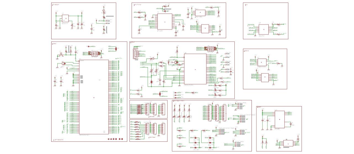
PCB schematic
2. PCB Schematic and PCB Design Software
From Protel to Altium
Anyone working in electronics knows Protel, just as computer users know the Windows operating system. Many of its operating habits have become deeply rooted in the industry.
Protel was a CAD software for the circuit industry released in the late 1980s by Protel (now Altium). It ranked among the top EDA tools and became the preferred software for circuit designers.
From early PCB design tools under DOS to the powerful Altium Designer today, Altium has released many versions. Commonly used versions include:
-
Protel 99SE
Although an early version, it is still widely used in many companies, including ours. Some companies only accept files in this format.
-
Protel 2004 SP4
Altium released Protel DXP in 2002. While some users remained loyal to Protel 99SE, many adopted Protel 2004 for its new features.
Later versions no longer used the “Protel” name, so this version is seen as a classic milestone. It is often used to open files that Protel 99SE cannot support.
-
Altium Designer 6.8
Altium officially released Altium Designer 6.0 in 2005, marking the end of the Protel era. Altium Designer 6.8 was released in 2007.
This software integrates all technologies required for integrated electronic product development, providing a unified platform for engineers. It covers board-level design, FPGA design, embedded software development, PCB layout, editing, manufacturing, and design data management. Tools such as P-CAD were gradually integrated into Altium Designer after 2006.
OrCAD and Cadence
OrCAD is an EDA software released in the late 1980s by OrCAD. It is well known as one of the best tools for schematic design.
Later, Cadence acquired OrCAD, enabling interactive design between OrCAD and Allegro. Many engineers use OrCAD (now Design Entry CIS) for schematics and Allegro for PCB layout, forming an ideal combination.
To accommodate user habits, Cadence integrated multiple tools into a unified environment. Today, the Cadence Allegro System Interconnect Design Platform mainly includes:
- Design Entry CIS (OrCAD) – schematic design
- Design Entry HDL – schematic design
- Allegro PCB Editor – PCB layout
- Allegro AMS Simulator – simulation
- Allegro PCB SI – signal integrity analysis
Cadence excels in high-speed signal simulation. As signal frequencies increase and boards become smaller, proper wiring alone is no longer sufficient. Signal integrity analysis has become essential. Tools such as the Constraint Manager in Allegro help engineers greatly optimize signal performance.
Beyond PCB design, Cadence also provides IC design tools, which will become essential knowledge for electronics engineers in the near future.
PADS / PowerPCB
Although PADS appeared later and was less well-known initially, it has been widely accepted by designers for its powerful functions, simple operation, and strong compatibility with PCB manufacturing. It became popular starting with PowerPCB 5.0.
The early PADS suite included PowerLogic (schematic), PowerPCB (PCB design), HyperLynx (signal analysis), and other tools.
The widely used PADS 2007 includes:
- DxDesigner – project management
- PADS Logic – schematic design
- PADS Layout – PCB design
- HyperLynx – signal integrity analysis
Today, PADS has become a complete and professional EDA solution for schematic design, PCB layout, high-speed signal analysis, and project management.

