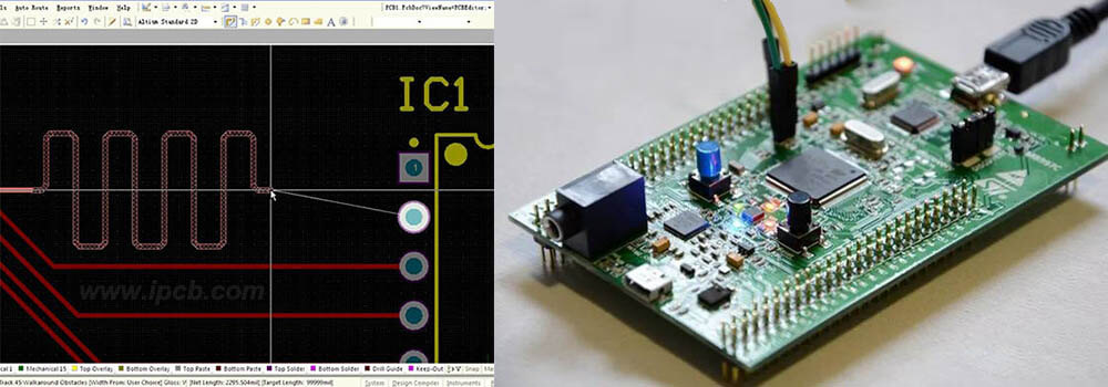
1. PCB Design
At Maxipcb, PCB design is fully customized around customer functional requirements. Our PCB design engineers develop detailed schematics to realize customer-specific tasks, focusing on external connection layout, product form factor, optimal component placement, circuit routing, via design, electromagnetic protection, and thermal management.
An excellent PCB design reduces manufacturing costs while significantly enhancing the performance and reliability of electronic products.
2. Maxipcb PCB Design Service
PCB design service is one of the key ways Maxipcb helps customers accelerate time-to-market. Our engineering team possesses extensive practical experience in optimizing PCB performance and manufacturability.
We specialize in PCB design for:
- Network Communication
- Industrial Control
- Medical Equipment
- Aerospace
- IC ATE Test
- Computer & Server
- Automotive Electronics
- Mobile Devices
3. What is PCB Design with MaxiPCB?
-
Whether you have only an idea, a concept, or a completed schematic, we can convert it into mature design documents and support subsequent PCB manufacturing, assembly, and testing.
With over 15 years of experience in printed circuit board manufacturing and assembly, we ensure designs are fully production-ready.
-
Maxipcb’s PCB design team collaborates with you throughout product development, conducting comprehensive technical reviews before mass production.
-
Once the design is approved for production, our professional manufacturing team quickly delivers high-quality PCBA prototypes for testing and validation.
-
Supporting both automated and manual assembly, we can populate PCBs in as fast as 48 hours, with standard full inspection and optional advanced testing.
-
Maxipcb provides one-stop integrated services to create a seamless process, saving you time so you can focus on bringing products to market.
4. Maxipcb Circuit Board Design – Premium Electronic Layout Artistry
Based on professional circuit board design and PCB prototyping, we provide a one-stop solution covering:
- PWB Design
- PCB Manufacturing
- SMT Assembly
- Material Supply
- Full PCBA Services
Senior PCB Design & Layout Team
- Over 15 years of professional design experience
- Provides end-to-end solutions from PCB design to PCBA manufacturing
- Balances design quality, cost control, and debugging convenience
Expertise in High-Difficulty PCB Design
We excel at:
- High-Frequency PCB
- High-Speed PCB
- High-Density Interconnect (HDI)
- Digital-Analog Mixed Circuits
- High-Power & High-Current Designs
- RF PCB
- ATE PCB
- Rigid-Flex PCB
- High-Speed Backplanes
We complete over 2,000 PCB design projects annually.
Strong Technical Resources
- Early cooperation with chip manufacturers
- Access to cutting-edge and forward-looking technologies
- Comprehensive consideration of EMI, EMC, and DFM design rules
Strict Quality Management System
- Standardized design management
- Multi-level strict inspection
- Zero-defect target
- Trusted by over 10,000 customers
High-Standard Confidentiality
- Confidentiality agreements signed for all projects
- Full encryption on designers’ computers
- Strict approval process for document export
- 100% intellectual property and data security
Quality Control System
- Complete design guidelines and specifications
- Additional technical support beyond layout
- Professional training system and platform
Self-Inspection
Covers layout, routing, design rules, aesthetics, thermal structure, and more.
Expert Review
Senior team conducts comprehensive reviews including:
- Schematic design
- DFM (Design for Manufacturability)
- DFT (Design for Test)
- High-speed signal integrity
- EMC performance
- Thermal design
Mutual Inspection
Avoids individual bias through brainstorming and a standardized joint review system, with a complete DFM review process.
|
|
PCB Design Parameter
Highest layers: 42L
Minimum line width: 2.4mil
Maximum number of pins: 110000+
maximum connection: 78000+
Minimum BGA pins spacing: 0.3mm
Maximum number of BGA-pins: 2912
Highest speed signal: 60GHZ
Minimum line spacing: 2.4mi
|
PCB Design delivery date
PIN Design delivery date
Within 1000: 3-5 days
2000-3000: 5-7 days
4000-5000: 8-12 days
6000-7000: 12-15 days
8000-9000: 15-18 days
10000-13000: 18-20 days
14000-15000: 20-22 days
16000-20000: 22-30 days
|
5. PCB Design Software
We use industry-leading EDA tools to ensure design accuracy and efficiency:
-
Altium Designer
Widely used in China, intuitive for general designs, suitable for a wide range of standard projects.
-
Cadence SPB (OrCAD)
International industry standard, powerful for schematic, PCB design, and simulation. Ideal for high-speed and complex designs.
-
Mentor EE
High-end platform comparable to Cadence SPB, with superior routing and automatic interconnection capabilities.
-
Eagle
Popular in Europe for its ease of use and efficient layout environment.
For professional and high-quality PCB design, Cadence SPB is strongly recommended for establishing robust design standards.
6. How We Design PCB Boards
Four Stages of PCB Design
-
Concept Refinement
Define project objectives and technical scope.
-
Feasibility Study
Evaluate technical and budget feasibility; provide a draft report for customer feedback.
-
Hardware & Software Design
Develop electronic circuits, schematics, and bench-top prototypes; draft firmware code.
-
Testing & Validation
Conduct rigorous bench testing until the design fully meets specifications.
Pre-Design Preparation
- Component library and schematic preparation
- Custom PCB footprint development based on official device specifications
- Strict matching between schematic symbols and PCB footprints
PCB Structure Design
- Define board outline and mechanical dimensions
- Place connectors, mounting holes, switches, and positioning components
- Reserve keep-out areas for assembly and heat dissipation
Core PCB Design Process
- Create schematics based on product functions
- Generate netlists
- Support direct netlist input for simple boards
- Adjust pin definitions and net assignments for reliability
PCB Layout
Special attention is paid to:
- Core and high-risk components
- High-voltage, high-power, and heat-generating devices
- Noise-sensitive and interference-prone circuits
- Board size optimization (balance between cost, impedance, heat dissipation, and anti-interference)
Proper layout ensures circuit functionality, signal integrity, and production stability.
7. PCB Prototype – Assembly – PCBA Testing
After design completion, we support:
- PCB prototyping
- Component procurement
- PCBA assembly
- Firmware programming
- Functional testing and optimization
This stage is critical to avoiding failures in mass production.
8. Maxipcb PCBA Design & Technology Advantages
- DFM (Design for Manufacturability)
- DFT (Design for Testability)
- DFA (Design for Assembly)
- High-density & backplane design
- Thermal optimization
- Stack-up design
- Signal Integrity (SI) simulation & analysis
- Power Integrity (PI) analysis
- EMC/EMI optimization
- Cost-down design
- Advanced EDA application
- IC package coordination
9. Main Product Categories We Serve
- Network Equipment
- Bluetooth & Wireless Communication Modules
- C/Ku Band Tuners
- Routers & Network Switches
- Digital Cameras & DVRs
- Laptop Motherboards
- DVB & Satellite Receivers
- Mobile Phones, Walkie-talkies
- DVD & Portable Visual Devices
- Other high-precision electronic products
10. Maxipcb PCB Design Service Advantages
-
Strong Technical Backing
Senior experts provide full technical guidance to ensure design quality.
-
Strict & Standardized Process
Mature processes minimize risks and ensure consistency.
-
Dedicated & Scalable Team
Experienced hardware and software engineers enable fast response to urgent demands.
-
Custom Internal Tools
Proprietary software platforms improve efficiency and shorten design cycles.
-
Cutting-Edge Technology
Closely follow industry trends and cooperate with leading chipmakers for high-end design capabilities.
About Maxipcb
Maxipcb is a professional PCB & PCBA manufacturer providing one-stop R&D and production solutions:
- PCB Design
- PCB Manufacturing
- PCB Assembly & PCBA
If you have a product idea or development project, please feel free to contact Maxipcb today.


