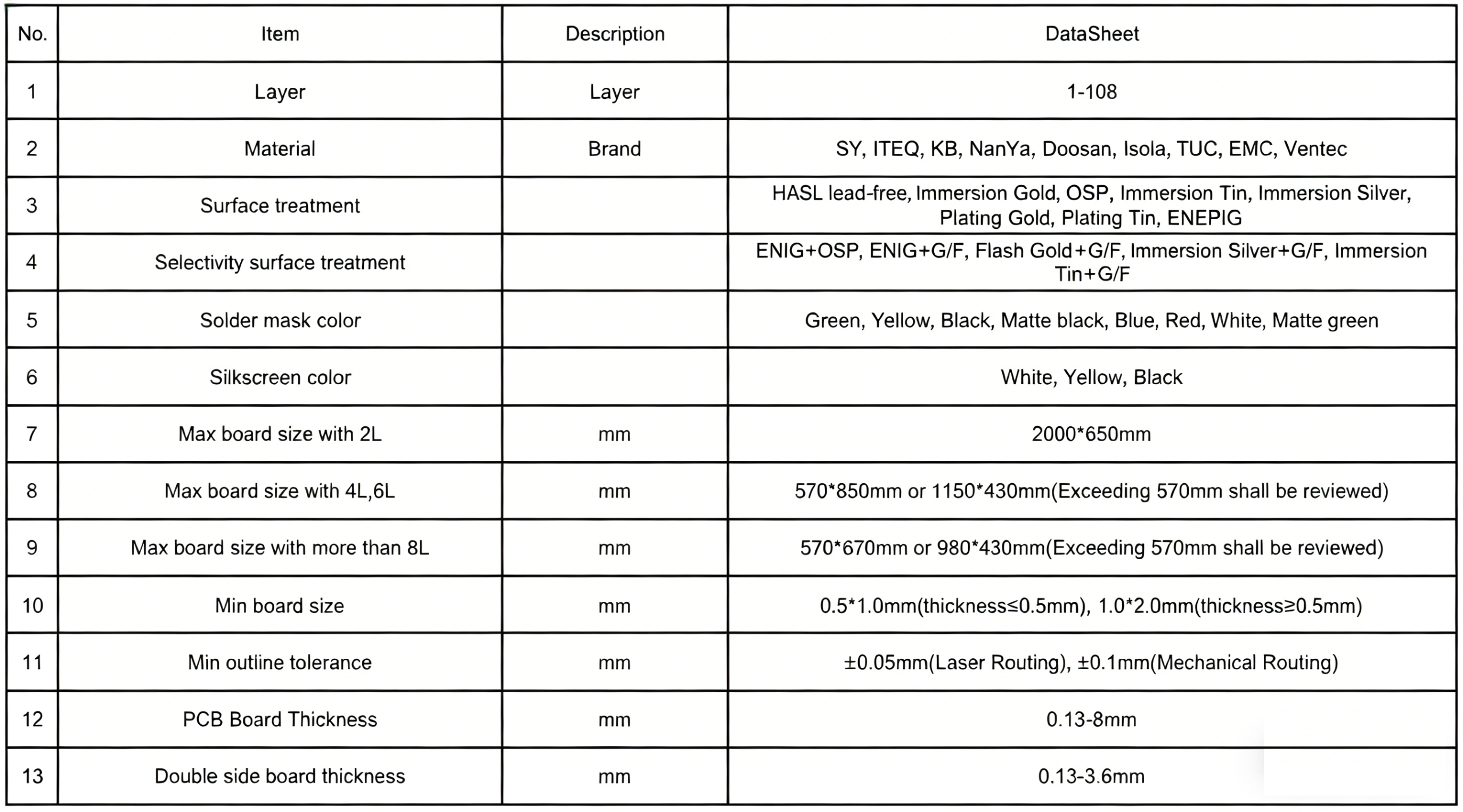
As the most widely used foundational printed circuit board in the global electronic manufacturing industry, FR-4 PCB is the core interconnect carrier for mainstream electronic products across all sectors. With 15 years of in-depth R&D and mass production experience in FR-4 PCB manufacturing, MaxiPCB is committed to providing global customers with high-quality, cost-effective full-range FR-4 PCB fabrication services. We have established a standardized full-process production management and control system, which serves as the core specification for order acceptance, contract review, DFM engineering design and mass production delivery, fully meeting the diversified needs of customers in various industries.
Core Product Coverage
Our FR-4 PCB manufacturing capabilities cover the full product matrix, supporting one-stop fabrication of conventional to high-end special structure boards:
- Conventional FR-4 PCB: Double-sided boards and multi-layer boards (2~36 layers), the mainstream mass production products with stable yield and fast delivery
- Ultra-high layer count FR-4 PCB: Stable mass production of 40~64 layer boards, with R&D and prototyping capability up to 108 layers
- Special structure FR-4 PCB: HDI blind & buried via PCB, multi-material mixed lamination PCB, metal core PCB, embedded component PCB
- Full compatibility: Support high-Tg, low-loss, high-reliability FR-4 substrates, and provide matching manufacturing services for high-frequency PCB, rigid-flex PCB and other special PCB products
Core Mass Production Capabilities
| Core Parameter |
Mass Production Capability |
Prototype & R&D Capability |
| Maximum Layer Count |
64 Layers |
Up to 108 Layers |
| Maximum Panel Size |
2000mm × 650mm (adjusted with layer count increase) |
2300mm × 700mm |
| Minimum Line Width/Line Spacing |
2mil/2mil (50μm/50μm) |
1mil/1mil (25μm/25μm) |
| Maximum Aspect Ratio (Through Hole Plating) |
24:1 |
Up to 48:1 |
| Impedance Control Tolerance |
±7% |
±3% |
| Supported Structures |
Standard multilayer PCB, blind & buried via PCB, mixed dielectric PCB, metal core PCB |
High-order HDI mixed lamination PCB, embedded component PCB, ultra-high layer count PCB |
Advanced Manufacturing Equipment & Process Control
To ensure ultra-high precision and batch consistency of products, we have deployed a full set of industry-leading advanced manufacturing equipment, and established a closed-loop process control system in strict accordance with IPC-A-600 and IPC-6012 international standards:
- Full-Process Laser Direct Imaging (LDI): Adopt LDI technology for both circuit pattern and solder mask fabrication, achieving micron-level precision control of line geometry, eliminating film deformation errors, and ensuring the consistency of fine line width and spacing in mass production
- Advanced Pulse Plating System: Equipped with high-throw pulse plating lines, achieving uniform copper plating in high-aspect-ratio through holes, ensuring interconnection reliability of ultra-high layer count boards, and supporting void-free blind hole filling plating with excellent surface flatness
- High-Precision Finishing Process: Adopt automated character inkjet printing technology, delivering clear, wear-resistant and high-contrast silkscreen graphics; provide a full range of surface treatment options including HASL, ENIG, ENEPIG, OSP, immersion silver/tin, to meet different SMT assembly requirements
- Full-Process Flatness Control: Optimized lamination and stress relief process for multi-layer boards, effectively controlling board warpage, ensuring excellent board flatness, and perfectly matching high-precision SMT assembly requirements of customers
2-Year Technology R&D Roadmap
To continuously lead the industry's technical development and meet the evolving needs of high-end electronic manufacturing, we have formulated a clear 2-year technology R&D roadmap, focusing on the following core directions:
- High-aspect-ratio pulse plating technology, targeting to achieve through-hole plating capacity with an aspect ratio of 48:1 and above
- Ultra-precision impedance control system optimization, targeting to reduce impedance control tolerance to ±3% and below
- Ultra-fine line manufacturing technology breakthrough, targeting to achieve stable mass production of 25μm/25μm (1mil/1mil) fine lines
- Continuous verification and mass production adaptation of new PCB materials, covering high-order HDI substrates, high-speed low-loss materials, IC substrate special materials, and ultra-thin high-precision application substrates
- High-aspect-ratio deep microvia manufacturing process R&D, targeting to achieve stable fabrication of microvias with an aspect ratio of 25:1 and above
- R&D of special substrate and via filling technology, including metal core PCB manufacturing process, conductive paste (Ormet, Tatsuta) and copper paste via hole plugging technology
- Process R&D of embedded component PCB, including embedded capacitor PCB, embedded resistor PCB and embedded magnetic component PCB
Quality Assurance & Compliance
- All products are manufactured in strict accordance with IPC-A-600, IPC-6012 Class 2/Class 3 international standards, with a full closed-loop quality management system covering raw material incoming inspection, in-process SPC statistical process control, and finished product reliability testing
- Professional DFM engineering team provides free pre-production design for manufacturability audit, optimizing design solutions, reducing production risks and improving product yield
- All products fully comply with RoHS, REACH and other global environmental regulations, supporting automotive-grade, industrial-grade, medical-grade and other high-reliability application scenarios
- With 15 years of industry accumulation, we have a stable core technical management team and a well-trained production workforce, ensuring stable batch consistency and an on-time delivery rate of over 98%