PCB Assembly Manufacturer

PCB Assembly Capability Hub

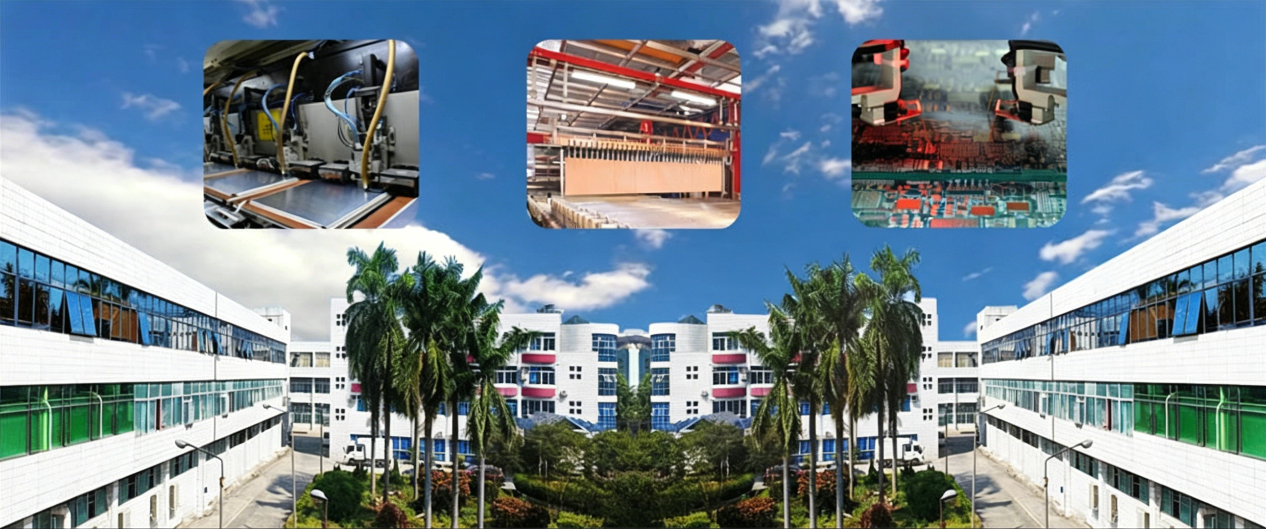
As a pcb assembly manufacturer that builds the bare board in-house as well, Maxipcb runs pcb assembly services end to end: NPI review, full BOM sourcing and verification, high-precision SMT, THT soldering, conformal coating and functional test — with a product conformity certificate travelling alongside every shipment.

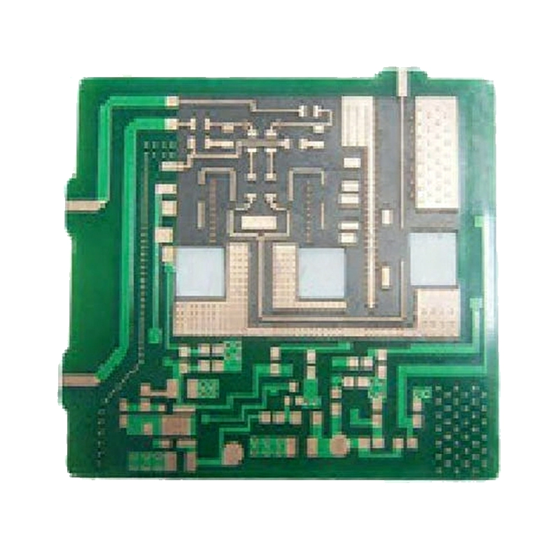
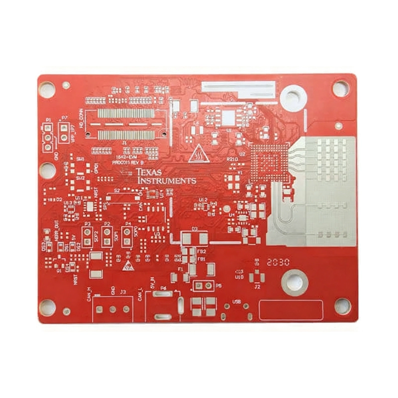
Custom printed circuit boards produced for an assembly build
2–64 Layers in mass production
2/2 mil Min line width & spacing
0.15 mm Min mechanical drill
24:1 Max aspect ratio
±5% Impedance control tolerance
UL · IATF16949 RoHS & REACH also covered

What Each Assembly Service Covers

Six hand-off points, each with the exact input that lets an engineer quote it without a follow-up call. Every card below stays inside documented assembly scope — nothing is subcontracted out of the route.

Service 01

Turnkey Build with Full BOM Sourcing

Your bill of materials is sourced through global mainstream component supplier channels and quality-verified before it reaches the line. Incoming material inspection sits ahead of every build, so what is kitted matches what is printed on your drawing.

Send us: BOM with reference designators, quantities, approved alternates and any manufacturer names you must keep.
Service 02

NPI Review & DFM Optimization

Every custom PCBA project is assigned a dedicated engineering project team. A pre-production NPI review meeting and full-process DFM optimization run across both fabrication and assembly before the first panel is released to production.

Send us: Gerber set, fabrication drawing, stack-up notes and your assembly drawing with polarity callouts.
Service 03

High-Precision SMT Assembly

The surface-mount stage is driven by high-precision SMT assembly and bracketed by DFM review upstream and AOI and X-Ray inspection downstream — so placement decisions are checked before reflow and again after it.

Send us: pick-and-place / centroid file with rotations, reference designators and board side.
Service 04

THT Soldering on the Same Route

Through-Hole Technology soldering runs inside the same build, so mixed-technology boards carrying both surface-mount and through-hole parts stay on one process route instead of being split between two suppliers.

Send us: through-hole component list with polarity, plus any height or clearance limits for the finished assembly.
Service 05

Conformal Coating

Conformal coating is a defined step in the PCBA flow rather than an afterthought, sequenced between soldering and final functional test so that coated boards still go through the full test gate before packing.

Send us: coating type, coverage areas, keep-clear zones and the connectors that must be masked.
Service 06

Functional Test & Test Fixtures

Customized functional test fixture development and test procedure formulation are part of the service, backed by AOI, X-Ray, ICT and FCT coverage and full-process quality control from incoming material inspection through to finished product functional testing.

Send us: your test specification, pass/fail limits and any customer-specific procedure you want implemented.

Assembly-Relevant Build Limits

This table is narrowed to the constraints that decide whether a design can be assembled and tested — not a reprint of the fabrication specification. Each row shows the mass-production figure first, then the extreme R&D prototype figure.

Parameter What we build to
Layer count 2–64 layers in mass production; up to 108 layers for extreme R&D prototypes.
Minimum line width / line spacing 2/2 mil (50/50 μm); 1/1 mil (25/25 μm) on prototype work.
Minimum mechanical drill hole 0.15 mm; 0.1 mm on prototype work.
Minimum laser blind via (HDI) 50 μm; 30 μm on prototype work.
Maximum aspect ratio 24:1; up to 48:1 on prototype work.
Impedance control tolerance ±5%; ±3% on prototype work.
Board thickness 0.15–8.0 mm multilayer and 0.10–8.0 mm double-sided; 0.08–10.0 mm on prototype work.
Minimum finished board size 0.5 mm × 1.0 mm, with customized ultra-small sizes available.
High-frequency hybrid lamination 4–32 layers; up to 40 layers on prototype work.
Surface finish HASL, ENIG, ENEPIG, OSP, immersion silver / tin, hard gold and customized special finishes.

Substrate selection, copper weight and the complete fabrication specification sit on the Custom PCB capability page.

Seven Stages, Seven Failures Prevented

The order of the route is not administrative — each gate exists because skipping it produces a specific, recurring defect.

1
DFM & NPI Review

Prevents: tooling spend on a build that cannot pass test.

2
Incoming Material Verification

Prevents: unverified components reaching the assembly line.

3
High-Precision SMT

Prevents: placement and reflow faults on dense layouts.

4
THT Soldering

Prevents: weak through-hole joints on mixed-technology boards.

5
Conformal Coating

Prevents: unprotected circuitry passing straight into final test.

6
AOI · X-Ray · ICT · FCT

Prevents: hidden solder and function faults escaping to you.

7
Conformity Certificate & Shipment

Prevents: boards arriving without traceable conformity records.

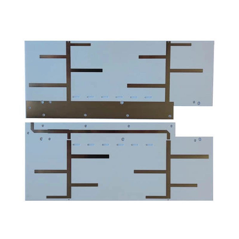
Custom PCB panel and circuitry prepared for assembly and test
Fabrication, assembly and test are handled by one team, so a non-conformance is traced back to a single process owner.

Quality, Compliance and Traceability

Compliance is only useful if it is documented per shipment, not per brochure. Here is what is held, what is checked and what travels with the box.

Standards followed

IPC-A-600, IPC-6012 and IPC-2221.

Compliance held

RoHS, REACH, UL and IATF16949.

Inspection coverage

AOI, X-Ray inspection, ICT (In-Circuit Test) and FCT (Functional Circuit Test), plus customized functional test fixture development and test procedure formulation.

Process control

Full-process quality control from incoming material inspection through to finished product functional testing, plus full BOM component sourcing and quality verification.

Traceability

Customer-specific test procedures and standards are supported with full implementation and traceability.

With shipment

Product conformity certification is provided with shipment.

Match Your Board to the Right Constraint

Find the build scenario closest to your product. The specification listed is the one that usually decides feasibility, cost and test strategy — and the input line tells you what to attach when you ask for a quote.

Wearable or handheld device

The deciding limits are usually density and thickness: HDI construction with laser blind vias down to 50 μm, board thickness from 0.15 mm, and finished board sizes down to 0.5 mm × 1.0 mm.

Send us: stack-up with via types, finished dimensions and the enclosure clearance envelope.

RF, radar or high-speed digital

Material choice drives the result: high-frequency and high-speed substrates are available in Rogers, Arlon, Taconic, Nelco, Isola, PTFE and hydrocarbon families, with hybrid lamination from 4 to 32 layers and impedance tolerance held to ±5%.

Send us: material callouts and impedance targets per net class.

Automotive-grade programme

Documentation matters as much as build quality: IATF16949 compliance, AOI / X-Ray / ICT / FCT coverage, and product conformity certification supplied with the shipment.

Send us: your test procedure plus the conformity documents your programme requires on file.

Medical or instrument board

Protection and repeatability lead here: conformal coating inside the assembly flow, full-process quality control from incoming material to finished-product functional testing, and traceability on customer-specific procedures.

Send us: coating and masking requirements together with the test procedure to be implemented.

LED or keyboard board

These sit in the industry-specific custom PCB range — custom LED PCB and custom keyboard PCB — built on the same 2–64 layer production window and 2/2 mil line and spacing capability.

Send us: Gerber, BOM and your panel or array requirements.

Dense mixed-technology assembly

Boards carrying both surface-mount and through-hole parts stay on one route, with aspect ratios up to 24:1 and surface finishes ranging from HASL through ENIG, ENEPIG, OSP, immersion silver / tin and hard gold.

Send us: pick-and-place data, the through-hole list and your preferred surface finish.

What to Send for an Assembly Quote

A complete pack shortens the NPI review and removes the clarification round. Send these seven items and the engineering team can quote assembly, test and tooling in one pass.

  • 01Gerber data for every layer, plus drill files.
  • 02BOM with reference designators, quantities and approved alternates.
  • 03Pick-and-place / centroid file showing rotations and board side.
  • 04Build quantity and required delivery schedule.
  • 05Test specification, pass/fail limits and any customer-specific procedure.
  • 06Stack-up and impedance requirements where the design is impedance-controlled.
  • 07Coating and masking requirements where conformal coating applies.

Request a Quote or a Custom PCBA Review

Send the pack to our team for material guidance, pricing and a quotation. Custom builds, repeat production runs and customer-specific test procedures are all handled by the same engineering group.

maxipcb@163.com

Related Reading

Three notes to help clarify product requirements before contacting the supplier.

Hybrid Lamination in Multilayer PCB Stackups With Mixed Materials

Hybrid lamination presses dissimilar laminates into one multilayer PCB, and the hard part is keeping expansion, resin flow, and layer registration under control.

Read article

HDI Microvia Structures in Compact Electronic Device Design

Compact devices squeeze more components and signals into less board area, and HDI microvia structures are how rigid boards keep up with that pressure.

Read article

Rigid-Flex PCB Bending Zones for Wearable and Medical Devices

Bending zones and rigid-to-flex transitions decide whether a wearable or medical rigid-flex board survives years of daily motion.

Read article

Frequently Asked Questions

what does the assembly scope actually cover?

turnkey assembly with full bom component sourcing and verification, a pre-production npi review with full-process dfm optimization, high-precision smt assembly, tht soldering, conformal coating, and functional test supported by aoi, x-ray, ict and fct.

can you source components for my bom?

yes. full bom component sourcing runs through global mainstream component supplier channels, with quality verification and incoming material inspection before the parts reach the line.

what test coverage do assembled boards receive?

aoi, x-ray inspection, ict and fct, together with customized functional test fixture development and test procedure formulation. customer-specific test procedures and standards are supported with full implementation and traceability.

which standards and compliance marks apply?

builds follow ipc-a-600, ipc-6012 and ipc-2221, with compliance stated for rohs, reach, ul and iatf16949. product conformity certification is provided with shipment.

what should i send for an assembly quote?

gerber and drill data, a bom with approved alternates, a pick-and-place file, your build quantity and schedule, the test specification with pass/fail limits, and any stack-up, impedance or coating requirements.

what build limits apply to layers, line spacing and vias?

mass production runs from 2 to 64 layers with 2/2 mil (50/50 μm) minimum line width and spacing, 0.15 mm minimum mechanical drill, 50 μm minimum laser blind via and a maximum aspect ratio of 24:1. extreme r&d prototypes extend to 108 layers, 1/1 mil spacing and 48:1 aspect ratio.