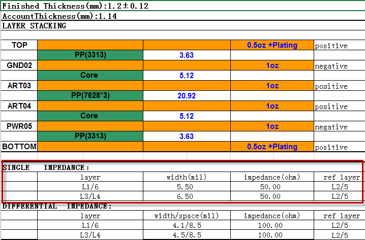
During PCB design, we typically define the layer stackup before routing, and calculate impedance based on parameters such as board thickness, base material, and layer count. The results are usually presented as shown in the figure below:
During PCB design, we typically define the layer stackup before routing, and calculate impedance based on parameters such as board thickness, base material, and layer count. The results are usually presented as shown in the figure below:
PCB Layer Stackup and Impedance Calculation Table
As can be seen from the figure above, single-ended networks in design are generally controlled to 50 ohms. Many people may ask: why specify 50 ohms instead of 25 ohms or 80 ohms?
First, 50 ohms is the default industry-accepted value, which stems from a recognized standard adopted by the entire industry.
A large portion of electronic technology originated from military applications; it was first used for military purposes and gradually transitioned to civilian use.
In the early days of microwave applications (during World War II), impedance selection was entirely based on application needs with no standard value. As technology advanced, a standardized impedance was required to balance cost and convenience.
In the United States, the most commonly used waveguides were assembled from existing scale rods and water pipes, making 51.5 ohms widespread. However, adapters and converters in use supported 50–51.5 ohms. To resolve these inconsistencies for the joint Army and Navy, an organization named JAN (later DESC) was established under the MIL standard. After comprehensive evaluation, 50 ohms was finalized as the standard. Corresponding waveguides were manufactured accordingly, and this standard was extended to various cables.
At that time, the European standard was 60 ohms. However, under the influence of industry-leading companies such as Hewlett-Packard, Europe was forced to adopt 50 ohms. Thus, 50 ohms became an industry standard and a convention. To achieve impedance matching, PCBs connected to various cables also adopted the 50-ohm impedance standard.
Second, the formulation of this standard is based on a comprehensive consideration of PCB manufacturing processes, design performance, and feasibility.
From the perspective of PCB manufacturing processes, producing PCBs with 50-ohm impedance is readily achievable with the equipment of most mainstream PCB manufacturers.
As shown in impedance calculations, excessively low impedance requires wide trace widths, thin dielectrics, or high dielectric constants, which are difficult to accommodate on high-density boards. Excessively high impedance requires narrow trace widths, thick dielectrics, or low dielectric constants, which impair EMI and crosstalk suppression and reduce processing reliability for multilayer boards and mass production.
Controlling 50-ohm impedance allows the use of common materials (e.g., FR4), standard core boards, and typical board thicknesses (e.g., 1 mm, 1.2 mm), with feasible trace widths (4–10 mils). This makes fabrication convenient for PCB manufacturers with low equipment requirements.
From the perspective of PCB design, 50 ohms is a balanced choice. For transmission line performance, lower impedance is generally preferable: for a given trace width, a closer distance to the reference plane reduces EMI and crosstalk.
However, from the perspective of the full signal path, the most critical factor is the driving capability of chips. Early chips could not drive transmission lines with impedance lower than 50 ohms, while higher impedance was impractical to implement. Thus, 50 ohms was adopted as a compromise.
Therefore, 50 ohms is generally selected as the default impedance for conventional single-ended signal control.
About Maxipcb
Maxipcb empowers innovators to turn cutting-edge technologies into reality.
We offer one-stop solutions for design, simulation, testing, PCB manufacturing, component procurement and SMT assembly, enabling efficient development, rapid deployment and risk control across the full product lifecycle.Serving the world in communications, industrial automation, aerospace, automotive, semiconductor and beyond, we build a safer, more connected future together.