In the past, FR-4 was universally used for PCB material selection without further consideration. As clock frequencies were low and signal rise times were slow in earlier designs, substrate performance did not cause issues. Today, operating frequencies frequently reach multiple gigabits per second with extremely fast edge rates and minimal timing margins, making precise material selection critical to product performance.
In the past, FR-4 was universally used for PCB material selection without further consideration. As clock frequencies were low and signal rise times were slow in earlier designs, substrate performance did not cause issues. Today, operating frequencies frequently reach multiple gigabits per second with extremely fast edge rates and minimal timing margins, making precise material selection critical to product performance.
Accordingly, control over the material selection process has become stricter. Materials used for multilayer PCB fabrication historically absorbed high-frequency signals and degraded edge rates, becoming a primary cause of signal integrity issues. However, not all designs target cutting-edge PCBs; over-specifying requirements can raise production costs unnecessarily.
Over the years, the industry has developed a vast array of materials for multilayer PCB manufacturing. The iCD dielectric material library currently offers over 700 rigid and flexible dielectric materials from more than 60 manufacturers. Selecting the appropriate material for each target application ensures PCB designs meet performance goals at the lowest possible cost.
Electromagnetic energy propagates at the speed of light in a vacuum or air. When confined within the dielectric material of a PCB, its propagation speed slows. Signal traces in a PCB merely guide electromagnetic waves as they travel through the surrounding dielectric. The propagation velocity (v) of electromagnetic energy is determined by the dielectric material:
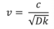
Where c is the speed of light (in free space), and Dk is the dielectric constant of the material (approximately 4.0 for FR-4). The Dk value of air is 1. Thus, electromagnetic energy propagates at roughly half the speed of light in FR-4, equivalent to 6 inches per nanosecond.
The electrical properties of dielectric materials are defined by two key parameters:
- Dielectric Constant (Dk) or Relative Permittivity (Er): The ratio of electromagnetic energy stored in the material under an applied voltage relative to that stored in a vacuum. This parameter describes how a material increases capacitance and slows electromagnetic wave propagation.
- Dissipation Factor (Df), Dielectric Loss, or Loss Tangent (tan δ): A measure of intrinsic electromagnetic energy dissipation within the dielectric material.
Dk and Df are independent of transmission line geometry; they are material properties governing signal propagation in PCB stackups at a given frequency. These properties cause frequency-dependent loss and reduce signal velocity. Impedance discontinuities and dielectric loss degrade signal quality received at the load.
FR-4, the common glass-epoxy PCB material, exhibits negligible loss in digital applications below 1 GHz. At higher frequencies, however, its loss causes severe performance issues.
Fast signal rise/fall times require high electromagnetic propagation speeds, which demand a sufficiently low Dk value. Materials with high Dk significantly reduce electric field strength within a given dielectric volume, making them ideal for concentrating electric fields and increasing inter-plane capacitance. High-speed designs therefore require low-Dk materials.
High-efficiency dielectric materials support charge transfer with minimal heat loss. Energy dissipation in dielectrics occurs via two mechanisms:
- Conductive Loss: Energy loss as charges flow through the material.
- Dielectric Loss: Energy dissipated as charges alternate direction with the changing electric field polarity.
Dielectric loss peaks near the resonant frequency of polarization mechanisms, as polarization lags the applied electric field, creating interactions that generate heat (Figure 1).
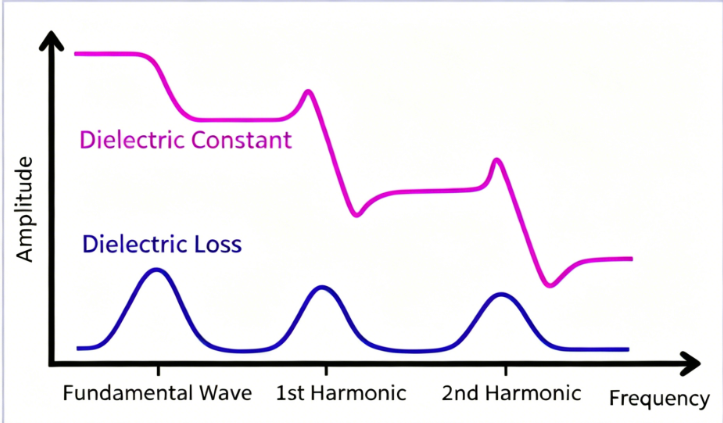
Figure 1 – Dielectric Constant and Dielectric Loss vs. Resonant Frequency
(Horizontal Axis: Frequency; Curves: Fundamental Wave, 1st Harmonic, 2nd Harmonic)
Temperature-related properties are also critical. The most important parameter is the Glass Transition Temperature (Tg), the temperature at which rigid glass transitions to amorphous resin/epoxy.
Prolonged exposure to reflow temperatures above Tg causes rapid Z-axis expansion and severe degradation of mechanical properties (reduced strength and bonding). High Tg prevents via barrel cracking and pad lift during reflow. Standard FR-4 has a Tg of 135–170°C, while high-speed materials typically exceed 200°C.
Decomposition Temperature (Td) is the temperature at which the material undergoes irreversible chemical breakdown. Most materials have a Td of 320°C, which is sufficient for standard processes.
Coefficient of Thermal Expansion (CTE) describes Z-axis expansion rate with increasing temperature; CTE should be as low as possible (<70 ppm).
Many other material properties must be considered, and manufacturers optimize material blends for high-speed designs. Conveniently, materials with low Dk also feature low Df, high Tg, and high Td—exactly the properties required for high-speed applications. Thus, Dk and Df are sufficient for initial material screening.
With hundreds of materials available, how to select the best fit for a specific product? Low cost often correlates with lower quality, but poor yield also increases total cost.
Dielectric material selection is primarily determined by digital signal frequency and rise time. High-frequency applications require low-loss materials, which typically have low Dk and enable faster signal propagation. Table 1 defines loss curve categories.
Table 1 – Loss Curve Ranges
| Loss Level |
Data Rate (Gbps) |
Frequency (GHz) |
Dissipation Factor (Df) |
| Ultra-Low Loss |
≥50 |
≤25 |
0.005 |
| Low Loss |
25–50 |
12.5–25 |
0.005–0.010 |
| Medium Loss |
10–25 |
5–12.5 |
0.010–0.015 |
| Standard Loss |
2–10 |
1–5 |
0.015–0.02 |
| Basic FR-4 |
— |
— |
≥0.02 |
Figure 2 plots loss curves for dielectric materials with Df < 0.005. The iCD Materials Planner includes five default curves spanning basic FR-4 to ultra-low-loss materials.
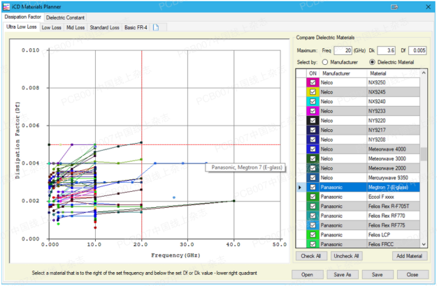
Figure 2 – Loss Curves of Ultra-Low-Loss Dielectric Materials (Source: iCD Materials Planner)
Material availability varies by region and manufacturer. Prototypes are usually fabricated locally, while mass production in Asia is more cost-effective. PCB fabricators’ material inventories should be mapped for side-by-side comparison.
Figure 3 shows loss performance of dielectric materials from an Asian manufacturer, allowing designers to select the best high-speed material from in-stock options at a glance. Cost-performance evaluation is essential to minimize material cost, noting that pricing varies with order quantity.
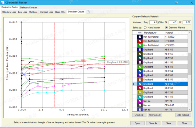
Figure 3 – Example Loss Curves of Dielectric Materials (Source: iCD Materials Planner)
Matching dielectric constant values is critical. Even small Dk variations between materials severely impact impedance, trace width, and spacing, leading to inconsistent losses. Dk directly determines signal propagation velocity; mismatched Dk between PCB layers causes timing errors. Designers should use drop-in materials to match impedance and Dk across all stackup layers.
PCB designers must quickly select materials with optimal performance and cost-performance from extensive options. Searching datasheets and specifications is inefficient. Visual comparison of dielectric materials—by manufacturer portfolio and, more importantly, by fabricator in-stock inventory—proves the most effective selection method.
Key Takeaways
- Multilayer PCB materials absorb high frequencies and degrade edge rates, a primary source of signal integrity issues.
- Appropriate material selection meets design and performance goals at minimum cost.
- Electromagnetic energy propagates at light speed in air/vacuum but slows in PCB dielectrics; FR-4 reduces speed to ~50% (6 inches/ns).
- FR-4 loss is negligible below 1 GHz but problematic at high frequencies.
- High-speed designs require low-Dk materials; high-Dk materials concentrate electric fields and increase inter-plane capacitance.
- Dk measures stored electromagnetic energy; Df measures intrinsic energy dissipation.
- Conductive loss stems from charge flow; dielectric loss stems from alternating polarization.
- Dielectric loss peaks at resonant frequencies, causing heat generation.
- Low-Dk materials inherently offer low Df, high Tg, and high Td for high-speed applications.
- Dk matching is critical; small variations disrupt impedance, timing, and loss.
About Maxipcb
Maxipcb empowers innovators to turn cutting-edge technologies into reality.
We offer one-stop solutions for design, simulation, testing, PCB manufacturing, component procurement and SMT assembly, enabling efficient development, rapid deployment and risk control across the full product lifecycle.Serving the world in communications, industrial automation, aerospace, automotive, semiconductor and beyond, we build a safer, more connected future together.
