Even the most confident designers often shrink back from RF circuits, as they pose significant design challenges and require specialized design and analysis tools. This article presents six tips to help you simplify any RF PCB design task and reduce workload stress!
Even the most confident designers often shrink back from RF circuits, as they pose significant design challenges and require specialized design and analysis tools. This article presents six tips to help you simplify any RF PCB design task and reduce workload stress!
01 Maintain Intact and Precise RF Shapes
Some severe errors as described above may result in poor circuit performance or even functional failure. To minimize errors, simplify RF design tasks, and improve productivity, PCB design tools can provide import control for complex copper shapes. For example, you can create usable copper shapes by controlling the layers in DXF files and remapping them to CAD electrical system layers.
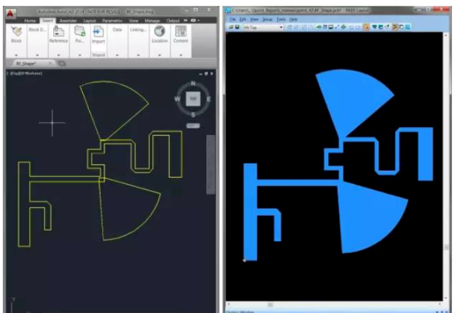
PCB design tools that allow users to control the DXF import process help reduce human errors and deviations, such as when imported files cannot be converted into copper shapes due to excessive complexity.
02 Retain Sharp Corners
An important aspect when designing copper shapes for RF and microwave applications is the ability to create Gerber files with sharp corners. Excellent PCB design tools can simplify this process. For instance, drawing shapes with 50mm lines typically results in smaller radii compared to drawing with 50mm round apertures. Design tools can automatically convert line widths correctly to achieve sharp corners when generating Gerber files.
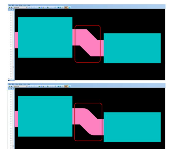
Effective PCB design tools automatically account for the line types used to draw shapes to calculate accurate line widths, helping you easily create sharp corners.
03 Automatic Chamfer Generation
Chamfers are frequently used in RF and microwave circuits to reduce the step discontinuity reactance between feedlines and capacitors, thereby improving the frequency performance of MMICs. The distance between 90° corners and chamfers is critical. Therefore, designers need an automated method to specify the chamfer ratio to be generated based on the design. PCB design tools that can automatically enforce the required chamfer ratio based on design rules benefit designers and engineers by saving time and improving design quality.
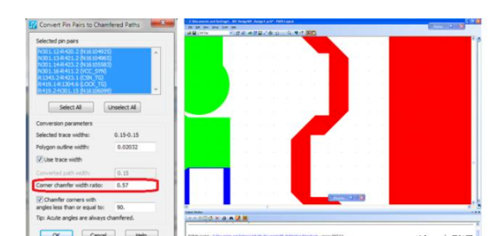
The function of setting chamfer rules simplifies the design process and saves time.
04 Automated Layout of Coplanar Waveguides and Channel Waveguides
Coplanar waveguides and channel waveguides are also common in RF and microwave design. Creating them manually is time-consuming and error-prone. Designers need to control specific distances between traces and vias, as well as between adjacent vias, to ensure the circuit meets design performance requirements. Design tools can assist in this regard by providing via usage control and automated via placement to reduce complexity and improve quality.
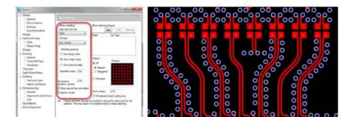
PCB design tools that enable control over the creation of coplanar waveguides and waveguide vias help significantly reduce design errors and shorten design cycles.
05 Use Automatic Stitching Vias
Another critical aspect of RF design is ensuring proper shielding of areas with vias. Although this task can be performed manually by designers, the process is extremely time-consuming. PCB design tools that can automate this process shorten design cycle times and ensure compliance with all your design rules. With such tools, designers can specify via pattern generation rules, leaving the rest to the PCB design tool.
06 Use Design Rules to Ensure "Right First Time" Design
PCB design tools supporting RF design typically allow configuration of multiple design rules: via types for different copper areas; net types to which vias must connect; required clearance from copper area edges to vias; distance from one via to the next; via pattern types; and whether a Faraday cage can be generated simply by adding vias to the outer edge of copper areas.
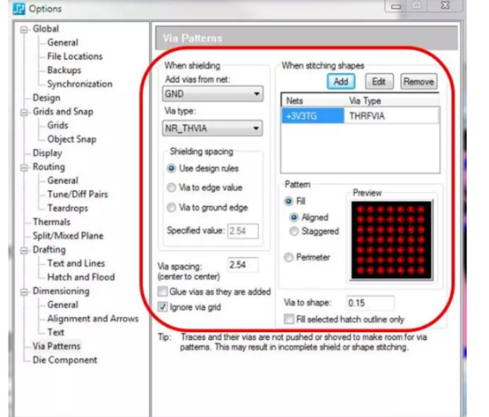
With RF-enabled PCB design tools, you can set design rules for via pattern generation and automatically enforce these rules in your design, saving time and ensuring compliance with all your design specifications.
About Maxipcb
Maxipcb empowers innovators to turn cutting-edge technologies into reality.
We offer one-stop solutions for design, simulation, testing, PCB manufacturing, component procurement and SMT assembly, enabling efficient development, rapid deployment and risk control across the full product lifecycle.Serving the world in communications, industrial automation, aerospace, automotive, semiconductor and beyond, we build a safer, more connected future together.
