Fiducial marks in PCB design refer to positioning markers commonly used to ensure accuracy and consistency during PCB manufacturing and assembly. These markers support automated positioning by operators and equipment during production, guaranteeing that all components are mounted at their correct positions. This is critical to ensuring product quality and reliability.
Fiducial marks in PCB design refer to positioning markers commonly used to ensure accuracy and consistency during PCB manufacturing and assembly. These markers support automated positioning by operators and equipment during production, guaranteeing that all components are mounted at their correct positions. This is critical to ensuring product quality and reliability.
This article explains in detail why fiducial marks must be placed after PCB design completion.
1. Improve Assembly Accuracy
Fiducial marks improve the precision of PCB assembly. For Surface Mount Technology (SMT), fiducial marks help assembly machines recognize the position and orientation of the PCB and perform automatic component positioning. They also help operators place components more easily at correct positions during manual assembly.
2. Enhance Manufacturing Efficiency
Fiducial marks improve PCB manufacturing efficiency. In the initial stage of board production, fiducial marks enable fast PCB positioning. Compared with manual position measurement, fiducial marks greatly reduce production time, boost efficiency, and shorten the manufacturing cycle.
3. Reduce Manufacturing Costs
Fiducial marks lower PCB manufacturing costs. By adding fiducial marks to the board, manufacturers can identify and locate the PCB more easily, reducing production expenses. They minimize costs caused by manual operation errors, further improving efficiency and cutting total manufacturing cost.
4. Lower Reflow Soldering Costs
Fiducial marks reduce reflow soldering costs. After components are mounted on the PCB, reflow soldering is an essential process. This process requires controlled temperature and time to ensure soldering quality and reliability. Fiducial marks enable automatic alignment of reflow soldering equipment, reducing defect rates and lowering reflow soldering cost.
5. Improve Board Stability and Reliability
Fiducial marks enhance the stability and reliability of the circuit board. These markers ensure accuracy and consistency throughout assembly and manufacturing, directly improving board reliability and stability. This is essential for producing high-quality, dependable products.
In summary, fiducial marks are an indispensable part of PCB design and are widely used in circuit board manufacturing and assembly. Adding fiducial marks to the PCB improves accuracy, consistency, and efficiency in assembly and production, reduces manufacturing costs, and enhances board stability and reliability.
Having explained the necessity of fiducial marks, we will now introduce their structural characteristics and design rules.
[Illustration: Fiducial mark style and dimensional requirements]
As shown in the figure, the fiducial mark structure consists of three elements:
- A central pad with a diameter of 1 mm;
- A solder mask opening with a diameter of 2 mm;
- An outer ring trace with a diameter of 3 mm.
The outer ring may be polygonal or circular; the two shapes have no functional difference and can be selected based on preference.
Fiducial Mark Placement Rules
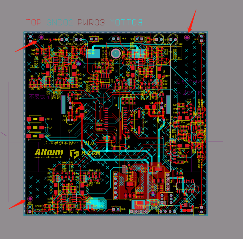
Fiducial marks are placed on the component‑mounting side. For single‑sided layouts, only one side requires fiducial marks. Typically, three fiducial marks are placed per side, near the board edges, usually at the corners, approximately 3 mm away from the board edge.
 About Maxipcb
Maxipcb empowers innovators to turn cutting-edge technologies into reality.
We offer one-stop solutions for design, simulation, testing, PCB manufacturing, component procurement and SMT assembly, enabling efficient development, rapid deployment and risk control across the full product lifecycle.Serving the world in communications, industrial automation, aerospace, automotive, semiconductor and beyond, we build a safer, more connected future together.
