interface signals operating at a rate of 8Gbps and above have stricter requirements for PCB routing design due to their extremely high speed. On the basis of the previous PCB routing content, the PCB routing design must also comply with the requirements specified in this article.
As shown in the table below, interface signals operating at a rate of 8Gbps and above have stricter requirements for PCB routing design due to their extremely high speed. On the basis of the previous PCB routing content, the PCB routing design must also comply with the requirements specified in this article.
| Interface |
High-Speed Differential Signals |
| DP1.4 8.1Gbps |
TYPECO_SSRX1P/DPO_TXOP; TYPECO_SSRX1N/DPO_TXON
TYPECO_SSTX1P/DPO_TX1P; TYPECO_SSTX1N/DPO_TX1N
TYPECO_SSRX2P/DPO_TX2P; TYPECO_SSRX2N/DPO_TX2N
TYPECO_SSTX2P/DPO_TX3P; TYPECO_SSTX2N/DPO_TX3N
TYPEC1_SSRX1P/DP1_TXOP; TYPEC1_SSRX1N/DP1_TXON
TYPEC1_SSTX1P/DP1_TX1P; TYPEC1_SSTX1N/DP1_TX1N
TYPEC1_SSRX2P/DP1_TX2P; TYPEC1_SSRX2N/DP1_TX2N
TYPEC1_SSTX2P/DP1_TX3P; TYPEC1_SSTX2N/DP1_TX3N |
| HDMI2.1 12Gbps |
HDMI_TXO_DOP/EDP_TXO_DOP; HDMI_TXO_DON/EDP_TXO_DON
HDMI_TXO_D1P/EDP_TXO_D1P; HDMI_TXO_D1N/EDP_TXO_D1N
HDMI_TXO_D2P/EDP_TXO_D2P; HDMI_TXO_D2N/EDP_TXO_D2N
HDMI_TXO_D3P/EDP_TXO_D3P; HDMI_TXO_D3N/EDP_TXO_D3N
HDMI_TX1_DOP/EDP_TX1_DOP; HDMI_TX1_DON/EDP_TX1_DON
HDMI_TX1_D1P/EDP_TX1_D1P; HDMI_TX1_D1N/EDP_TX1_D1N
HDMI_TX1_D2P/EDP_TX1_D2P; HDMI_TX1_D2N/EDP_TX1_D2N
HDMI_TX1_D3P/EDP_TX1_D3P; HDMI_TX1_D3N/EDP_TX1_D3N |
| PCI-E3.0 8Gbps |
PCI-E30_PORTO_TXOP; PCI-E30_FORTO_TXON
PCI-E30_PORTO_TX1P; PCI-E30_PORTO_TX1N
PCI-E30_PORTO_RXOP; PCI-E30_PORTO_RXON
PCI-E30_PORTO_RX1P; PCI-E30_PORTO_RX1N
PCI-E30_PORT1_TXOP; PCI-E30_PORT1_TXON
PCI-E30_PORT1_TX1P; PCI-E30_PORT1_TX1N
PCI-E30_PORT1_RXOP; PCI-E30_PORT1_RXON
PCI-E30_PORT1_RX1P; PCI-E30_PORT1_RX1N |
For high-speed signal routing, layer transition via drilling should be minimized. When layer transition is necessary, priority shall be given to layers with GND planes on both sides. Transmit and receive signals should be routed on different layers as much as possible. If space is limited and transmit and receive signal traces have to be routed on the same layer, the routing spacing between transmit and receive signals shall be increased.
The following additional requirements apply to the above high-speed signals:
01 Hollowing Out the Reference Layer in the BGA Pad Area
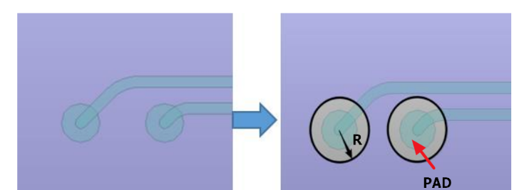
If the operating rate of the interface is ≥8Gbps, it is recommended to hollow out the L2 reference layer directly below these signals in the BGA area to reduce the capacitive effect of the pads, with a hollowed-out radius R=10mil.
If the operating rate of the interface is <8Gbps, for example, a DP interface only operating at 5.4Gbps, there is no need to hollow out the reference layer in the BGA area, as shown in the figure below.
02 Avoiding Fiberglass Weave Effect
The PCB substrate is formed by laminating glass fiber and epoxy resin filling. The dielectric constant of glass fiber is about 6, while the dielectric constant of resin is generally less than 3. The problems in path length and signal speed are mainly caused by the weaving method of glass fiber reinforcement in the resin.
In ordinary glass fiber weaving, the glass fiber bundles are tightly twisted together, so a large number of gaps left between the bundles need to be filled with resin. The average wire width in the PCB is smaller than the spacing between the glass fibers. Therefore, for a differential pair, one line may have more parts over the glass fiber and fewer parts over the resin, while the other line is the opposite (more parts over the resin than over the glass fiber). This will result in different characteristic impedances of the D+ and D- traces, as well as different time delays of the two traces, leading to intra-pair delay difference of the differential pair and thus affecting the quality of the eye diagram.
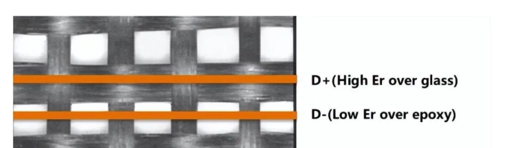
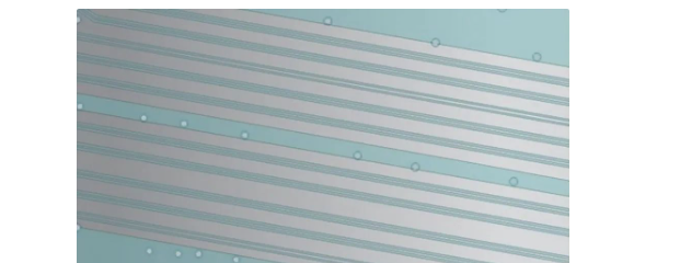
When the signal rate of the interface reaches 8Gbps and the trace length exceeds 1.5 inches, the fiberglass weave effect must be handled carefully. It is recommended to use one of the following methods to avoid the impact of the fiberglass weave effect:
Method 1: Change the routing angle, such as 10°~35°, or rotate the substrate by 10° during PCB production and processing to ensure that all traces are not parallel to the glass fiber, as shown in the figure below.
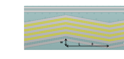
Method 2: For the routing shown in the figure below, W shall be at least 3 times greater than the fiberglass weave spacing, with recommended values of W=60mil, θ=10°, L=340mil.
03 Recommendations for Differential Vias
- For high-speed signals, layer transition via drilling should be minimized. When changing layers, GND vias must be added next to the signal vias. The number of ground vias has different impacts on the signal integrity of differential signals. The signal integrity of differential signals can be improved sequentially with no ground via, single ground via, and double ground vias.
- Select a reasonable via size. For the PCB design of general density multilayer boards, vias with 0.25mm/0.51mm/0.91mm (drill hole/pad/POWER isolation area) are preferred; for some high-density PCBs, vias with 0.20mm/0.46mm/0.86mm can also be used, and blind and buried via design can also be attempted.
- The change of the center-to-center spacing of vias has different impacts on the signal integrity of differential signals. For differential signals, excessively large or small center-to-center spacing of vias will adversely affect signal integrity.
- If the operating rate of the interface is ≥8Gbps, the via size of the differential pairs of these interfaces is recommended to be simulated and optimized according to the actual stack-up.
| Scheme |
D1(mil) |
D2 (mil) |
D3(mil) |
Differential Via Impedance |
| 1 |
26 |
18 |
22~26 |
100ohm |
| 2 |
24 |
18 |
22~26 |
95ohm |
| 3 |
22 |
18 |
22~26 |
90ohm |
| 4 |
22 |
15 |
22~26 |
- |
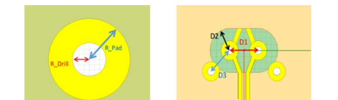
The reference via dimensions based on the EVB first-order HDI stack-up are given below:
R_Drill=0.1mm (drill hole radius)
R_Pad=0.2mm (via pad radius)
D1: center-to-center spacing of differential vias
D2: anti-pad size from the top layer to the bottom layer
D3: center-to-center spacing between signal vias and return ground vias
04 Recommendations for Coupling Capacitor Optimization
- The placement of coupling capacitors shall follow the requirements of the design guide. In the absence of a design guide, if the signal is transmitted from IC to IC, the coupling capacitor shall be placed close to the receiving end; if the signal is transmitted from IC to connector, the coupling capacitor shall be placed close to the connector.
- Select the package size as small as possible to reduce impedance discontinuity.
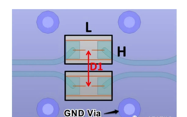
- If the signal operating rate of the interface is ≥8Gbps, the DC blocking capacitors of the differential pairs of these interfaces are recommended to be optimized as follows:
- Select to hollow out one or two ground planes according to the interface. If the L2 ground reference layer directly below the capacitor pad is hollowed out, layer-to-layer reference is required, that is, the L3 layer shall be the ground reference layer;
- If the L2 and L3 ground reference layers are hollowed out, the L4 layer shall be the ground reference layer. The hollowed-out size shall be determined by simulation according to the actual stack-up; the reference dimensions based on the EVB first-order HDI stack-up are given below.
【Note】D1: center-to-center spacing between differential coupling capacitors; L: hollowed-out length; H: hollowed-out width.
| Interface |
Hollowed-out Layer |
D1 |
H |
L |
Placement Position |
| DP1.4 |
L2 and L3 layers |
25mil |
20mil |
Equal to the pad length |
Close to the connector |
| HDMI2.1 |
L2 and L3 layers |
25mil |
20mil |
Equal to the pad length |
Close to the connector |
| PCI-E3.0 |
L2 layer |
25mil |
20mil |
Equal to the pad length |
Equal to the pad length |
- Place 4 ground vias around the coupling capacitor to connect the ground reference layers from L2 to L4, as shown in the figure below.
05 Recommendations for ESD Optimization
- The parasitic capacitance of the ESD protection device must be low enough to allow high-speed signal transmission without degradation.
- The ESD device shall be placed before the protected IC, but as close as possible to the PCB side of the connector/contact; before any resistor in series with the signal line; before filtering or conditioning devices including fuses.
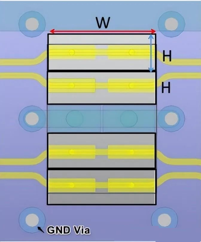
- If the signal operating rate of the interface is ≥8Gbps, the ESD devices for the differential pairs of these interfaces are recommended to be optimized as follows. Hollow out the L2 and L3 ground reference layers directly below the ESD pad, with the L4 layer as the layer-to-layer reference layer, which must be a ground plane. The hollowed-out size shall be determined by simulation according to the actual stack-up combined with the ESD model.
The reference dimensions for ESD model ESD73034D based on the EVB first-order HDI stack-up are given below:
| Interface |
Hollowed-out Layer |
H |
W |
| DP1.4 |
L2 and L3 layers |
22mil |
Equal to the pad length |
| HDMI2.1 |
L2 and L3 layers |
22mil |
Equal to the pad length |
- At the same time, place 4 ground vias around each ESD device to connect the ground reference layers from L2 to L4, as shown in the figure below.
06 Recommendations for Connector Optimization
- The traces inside the connector shall be led out from the center of the pins. If a high-speed signal has no adjacent GND pin at one end of the connector, a GND via shall be added next to it during design.
- If the signal operating rate of the interface is ≥8Gbps, the connector of these interfaces shall meet the corresponding standard requirements (such as HDMI 2.1/DP1.4/PCI-E3.0 protocol standards). Connectors from manufacturers such as Molex, Amphenol, HRS, etc. are recommended.
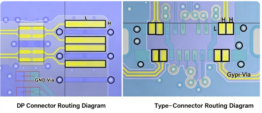
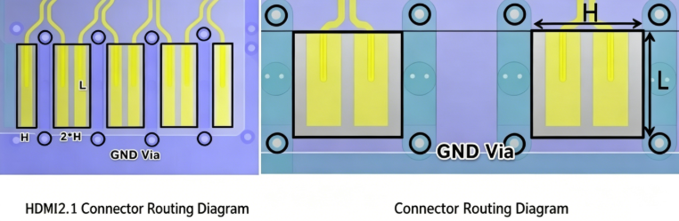
- Select to hollow out one or two ground planes according to the interface. If the L2 ground reference layer directly below the connector pad is hollowed out, layer-to-layer reference is required, that is, the L3 layer shall be the ground reference layer; if the L2 and L3 ground reference layers are hollowed out, the L4 layer shall be the ground plane as the layer-to-layer reference layer. The hollowed-out size shall be determined by simulation according to the actual stack-up combined with the connector model.
- It is recommended to place 2 ground vias for each ground pad of the connector, and the ground vias shall be as close to the pad as possible.
The reference hollowed-out dimensions based on the EVB first-order HDI stack-up are given below:
| Connector |
Model |
Hollowed-out Layer |
H |
L |
| DP |
Molex472720029 |
L2 and L3 layers |
18mil |
Equal to the pad length |
| Type-C |
Molex1054500101 |
L2 and L3 layers |
20mil |
Equal to the pad length |
| HDMI2.1 |
Molex2086581051 |
L2 and L3 layers |
20mil |
Equal to the pad length |
| PCI-E3.0 |
Amphenol 10076266-101TLF |
L2 layer |
- |
- |
Recommended Routing Methods for Connectors:
About Maxipcb
Maxipcb empowers innovators to turn cutting-edge technologies into reality.
We offer one-stop solutions for design, simulation, testing, PCB manufacturing, component procurement and SMT assembly, enabling efficient development, rapid deployment and risk control across the full product lifecycle.Serving the world in communications, industrial automation, aerospace, automotive, semiconductor and beyond, we build a safer, more connected future together.