The Key to PCB Layout: Should the Length of Switching Node Traces Be Minimized as Much as Possible? We believe many people have doubts about this, and today Maxipcb will answer this question for you!
The switching node of a switching regulator or power converter circuit is a critical conduction path that requires special attention during PCB layout. This circuit node connects one or more power semiconductor switches (such as MOSFETs or diodes) to magnetic energy storage devices (such as inductors or transformer windings). Its switching signal contains rapidly switching dV/dt voltage and dI/dt current, which can easily couple to surrounding circuits and cause noise problems, potentially resulting in the PCB and system failing to meet stringent electromagnetic compatibility (EMC) requirements.
This article will introduce the most basic switching node waveforms, help you understand how to determine the appropriate trace size for the switching (SW) node during PCB routing, and explain the near-field coupling effects generated by the electric field (E-field) and magnetic field (H-field) in the switching node.
Minimize the Length of Switching Node Traces as Much as Possible
Switching node traces need to carry relatively large time-varying currents over short distances. The inductor should be placed very close to the SW pin of the regulator. The shorter the wiring, the lower the coupling from the high-frequency electric field of the high dV/dt waveform and the low-frequency magnetic field from the inductor ripple current.
Figure 1 shows a routing example of the switching node, where the inductor is placed close to the regulator. When designing the PCB layout, attention should be paid to reserving a small area between the converter and the inductor for other components that must be connected to the switching node (such as a small bootstrap capacitor). However, the layout principle is to minimize the trace length of the SW node as much as possible.
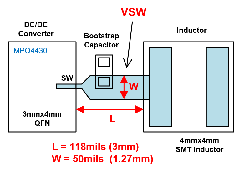
Figure 1: Switching Node Layout of a 3A Buck Converter on a 4-Layer PCB
Figure 1 shows that the placement principle of the bootstrap capacitor is to make its longest side perpendicular to the SW trace. This can reduce the unnecessary distance between the SW pin and the inductor. Although the capacitor pushes the inductor slightly further away, an ultra-short trace of about 3mm to 4mm can still be achieved. The specific VSW trace length depends on the application and component size, and may be longer than this example in some cases.
In summary, we believe that through the description in this article, you all have a certain understanding of the key to PCB layout: minimizing the length of switching node traces as much as possible. If you have any questions or want to know more, you can consult MaxiPCB.
About Maxipcb
Maxipcb empowers innovators to turn cutting-edge technologies into reality.
We offer one-stop solutions for design, simulation, testing, PCB manufacturing, component procurement and SMT assembly, enabling efficient development, rapid deployment and risk control across the full product lifecycle.Serving the world in communications, industrial automation, aerospace, automotive, semiconductor and beyond, we build a safer, more connected future together.
