In modern high-performance electronic devices, heat dissipation is a common and critical issue. Proper handling of heat dissipation is essential to ensure the reliability, stability and service life of electronic devices.
In modern high-performance electronic devices, heat dissipation is a common and critical issue. Proper handling of heat dissipation is essential to ensure the reliability, stability and service life of electronic devices.
The following will introduce the methods and techniques for handling heat dissipation issues in the PCB design process, to help you improve the quality and performance of your designs.
First of all, before addressing heat dissipation issues, it is necessary to accurately define and identify the heat generation sources. For example, specific components such as processors and power amplifiers usually generate a large amount of heat, which helps to clarify the heat management measures that need to be taken.
After identifying the heat sources, we then need to perform optimization during the layout process. Place components that generate a large amount of heat in appropriate positions on the PCB for better heat dissipation. Meanwhile, reserve a certain space around heat-generating devices, and avoid clustering high-power components together to prevent mutual hot spot effects. During layout, heat dissipation channels should also be reasonably allocated to ensure that hot air can flow out of the device smoothly. This can be achieved by arranging the positions of components and heat sinks, as well as optimizing the design of the device housing and ventilation openings.
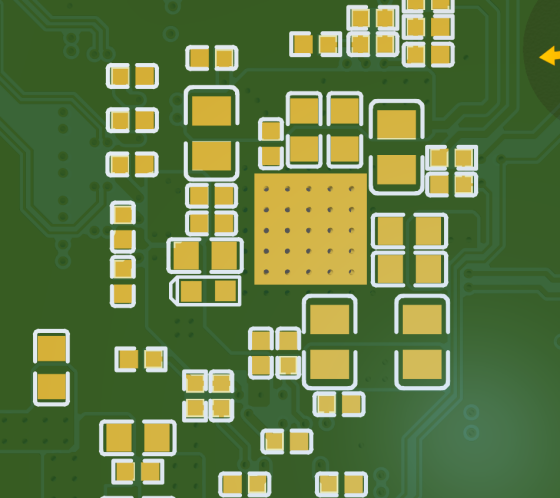
After the layout is completed, special treatment is also required during the routing process. For example, when handling a PMU (Power Management Unit) module, we need to ensure that multiple ground vias are placed at the thermal pad of the chip. In the case of a multilayer board, large-area copper pours on multiple layers can be provided in the PMU area to assist heat dissipation. Multilayer boards can achieve better heat distribution, thereby reducing heat concentration on the entire PCB.
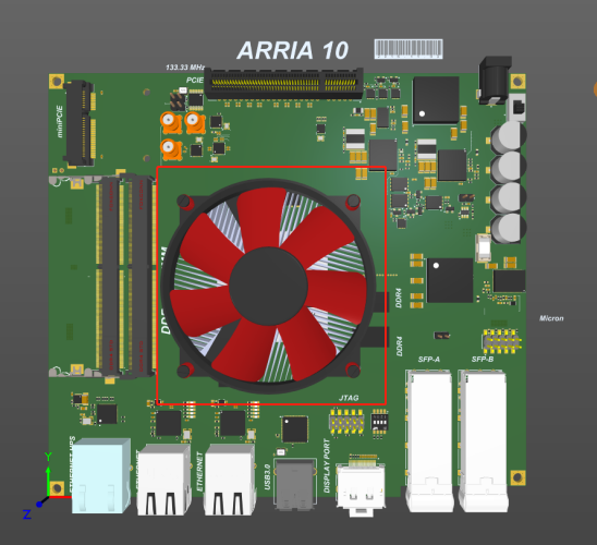
Of course, we can also perform window opening treatment on the thermal pad on the back side of the PMU. Attention shall be paid to maintaining a certain distance between the window opening area and the device as well as other networks to avoid short circuits. If the heat generation is still particularly severe, a thermal conductive pad and thermal grease can be placed on the back side to assist heat dissipation. The main control chip usually also generates extremely high heat; we can apply thermal grease on the main control chip, and use a fan to assist heat dissipation.
In addition, to achieve better temperature control, we can add thermistors in the PCB design to monitor the temperature, and adopt protection measures such as temperature control switches, to ensure that the circuit can operate normally at high temperatures and avoid damage.
In the heat dissipation design of PCBs, measures such as optimized layout, addition of heat sinks, use of thermal conductive materials, rational design of multilayer structures, ensuring air circulation, and increasing heat dissipation channels shall be considered, to improve heat dissipation efficiency and ensure the normal operation and service life of electronic devices.
About Maxipcb
Maxipcb empowers innovators to turn cutting-edge technologies into reality.
We offer one-stop solutions for design, simulation, testing, PCB manufacturing, component procurement and SMT assembly, enabling efficient development, rapid deployment and risk control across the full product lifecycle.Serving the world in communications, industrial automation, aerospace, automotive, semiconductor and beyond, we build a safer, more connected future together.