High-Density Interconnector (HDI) is increasingly widely used in the electronics industry, especially under the current trend of miniaturization of electronic products. For the same product, the selection of HDI designs with different structures will have a significant impact on the cost.
High-Density Interconnector (HDI) is increasingly widely used in the electronics industry, especially under the current trend of miniaturization of electronic products. For the same product, the selection of HDI designs with different structures will have a significant impact on the cost.
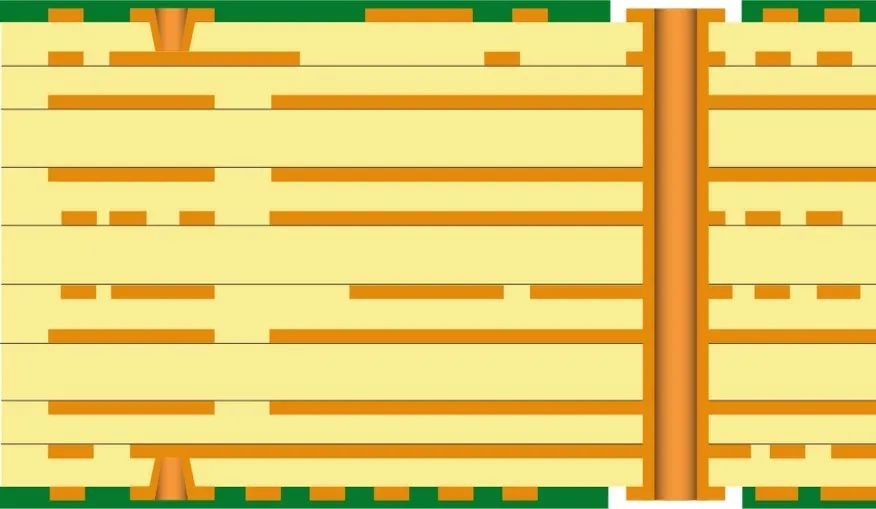
The figure above shows a 10-layer PCB with Type I HDI structure. The addition of two layers of micro vias means more laser drilling operations.
Compared with the standard structure, the cost increases by 40%-70%.
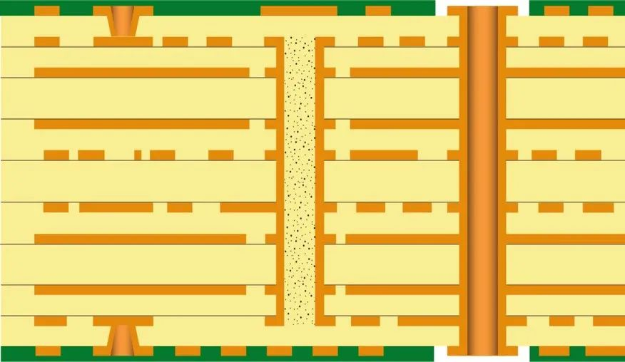
The figure above shows a 10-layer PCB with Type II HDI structure. The added buried via structure means more drilling, electroplating and lamination procedures.
Compared with the standard structure, the cost increases by 80%-120%.
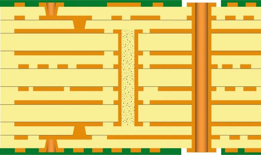
The figure above shows a 10-layer PCB with Type III HDI structure. More buried via structures mean more drilling operations (4 times), more electroplating processes (3 times) and more lamination steps (3 times).
Compared with the standard structure, the cost increases by more than 180%-200%.
Do you think the above cost fluctuation ranges for HDI with different structures are accurate?
The answer is no.
The cost fluctuation mentioned above does not take into account changes in the number of PCB layers or board dimensions, which are all key factors that will change after the introduction of the HDI structure. Different products have different designs, and the more complex the design, the greater the impact on the cost.
About Maxipcb
Maxipcb empowers innovators to turn cutting-edge technologies into reality.
We offer one-stop solutions for design, simulation, testing, PCB manufacturing, component procurement and SMT assembly, enabling efficient development, rapid deployment and risk control across the full product lifecycle.Serving the world in communications, industrial automation, aerospace, automotive, semiconductor and beyond, we build a safer, more connected future together.