Efficiently solve the radiation problem caused by ground split?
For various design requirements, ground split design is often adopted in PCB layout, such as:
- Digital signals are usually high-speed and high-frequency signals with high-frequency interference noise, while analog signals such as those in the power supply section are often low-frequency and large-current signals. High-frequency interference coupled into power supply signals is easily brought out of the board through cables such as power lines, resulting in radiation. The small analog signals collected by some sensors usually have a small amplitude, and high-frequency interference coupled into them can easily lead to signal state disorder, which will cause even more unpredictable consequences after amplification. Therefore, separate design of digital ground and analog ground is usually adopted.
- The drive output terminals of some motors have large broadband interference due to high-power, large-current and fast-switching drive signals. It is also necessary to split the ground of the power terminal from the ground of the front-end control signal, to prevent the noise from the drive terminal from coupling to the front end and interfering with the control signal, or being brought out from the control terminal and causing EMI problems.
- For the chassis ground and PCB ground of some products, ground split design is also adopted sometimes out of safety regulations and other considerations.
In the daily rectification work of Bichuangda, we often encounter EMI or EMS problems caused by ground split issues. After positioning and rectification by experienced on-site rectification engineers, the problems can be quickly solved through simple measures such as canceling the ground split or adding stitching capacitors. A classic case is shared as follows:
I. Overview of Ground Split Design
As mentioned at the beginning of the article, to reduce mutual coupling interference, split design is adopted for the analog ground and digital ground on the board.
As shown in Figure 1, if single-point grounding is adopted, or the analog part and the digital part share a common ground, there will always be a certain impedance in the ground return path (Lp and Rp in the figure are parasitic inductance and parasitic resistance respectively). At low frequencies, the impedance is low and the impact is insignificant, but at high frequencies, the impedance will be much higher. Due to the existence of ground impedance, an electromotive force will be generated when the loop current flows through, and the ground electromotive force will be lifted, thereby affecting the level of each module, which is the so-called ground bounce effect.
In Figure 1, the loop impedance of the analog part includes not only Z1 composed of Lp1 and Rp1, but also Z2 composed of Lp2 and Rp2 of the digital loop superimposed. Therefore, the analog part is more affected by ground bounce (V1+V2) than the digital part. At the same time, the high-frequency noise of the digital part will also be introduced into the analog part due to the common ground problem, thereby affecting the EMI performance of the product.
V1 =i1 × (jωLp1 + Rp1) (1)
V2 =(i1+i2) × (jωLp2 + Rp2) (2)
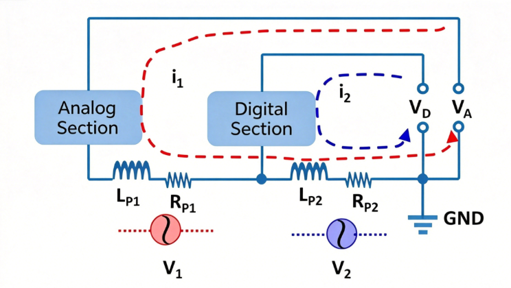
Figure 1 Schematic Diagram of Common Ground and Ground Bounce Effect
For EMI problems caused by the ground bounce effect, a commonly used solution is ground split design. As shown in Figure 2, it is a schematic diagram of ground split processing, where the digital ground and analog ground are separated. The grounds of digital signals, power supplies and analog signals, power supplies are connected to the digital ground and analog ground respectively, and then the digital ground and analog ground are bridged at a single point or multiple points. The bridge can be directly connected by copper foil traces, or by LRC filters (e.g. BTREF2012A2R601) or 0-ohm resistor shorting.
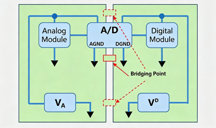
Figure 2 Schematic Diagram of Digital-Analog Ground Split
In addition, another cross-split situation is that high-speed traces cross the power split gap. As shown in Figure 3, if the high-speed traces use the power plane as the reference plane, there may be a cross-split problem caused by crossing different power regions. For this situation, stitching capacitors can be added near the cross-split area to ensure the continuity of the return path. The stitching capacitor method was adopted to solve the RE problem of the network card product mentioned in Section 1.
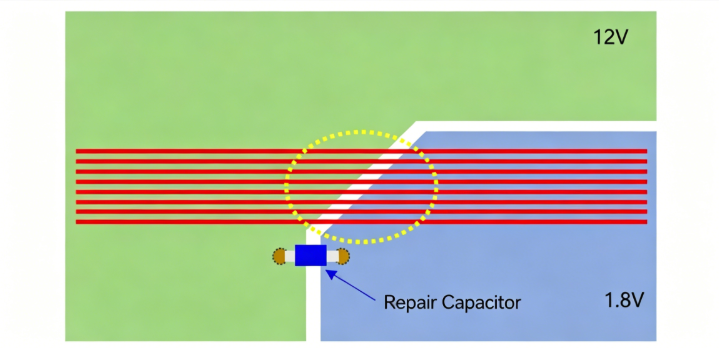
Figure 3 Schematic Diagram of Traces Crossing Power Planes and Stitching Capacitors
II. Summary
01 Ground split layout is an effective means to solve EMC problems, as well as SI (Signal Integrity) and PI (Power Integrity) issues. At the same time, it is mandatory for ground split in some application scenarios such as safety regulation requirements.
02 Ground split will inevitably cause problems such as impedance discontinuity and trace cross-split, so additional remedial measures are sometimes required, such as bead isolation bridging and stitching capacitor bridging.
About Maxipcb
Maxipcb empowers innovators to turn cutting-edge technologies into reality.
We offer one-stop solutions for design, simulation, testing, PCB manufacturing, component procurement and SMT assembly, enabling efficient development, rapid deployment and risk control across the full product lifecycle.Serving the world in communications, industrial automation, aerospace, automotive, semiconductor and beyond, we build a safer, more connected future together.
