After the PCB goes through the standard manufacturing process, the bare copper on the PCB is ready for surface finishing. PCB plating is used to protect any exposed copper on the PCB through the solder mask, whether it is pads, vias, or other conductive elements. Designers usually default to tin-lead (SnPb) plating, but other plating options may be more suitable for your board application.
After the PCB goes through the standard manufacturing process, the bare copper on the PCB is ready for surface finishing. PCB plating is used to protect any exposed copper on the PCB through the solder mask, whether it is pads, vias, or other conductive elements. Designers usually default to tin-lead (SnPb) plating, but other plating options may be more suitable for your board application.
In this article, I will introduce different PCB plating material options and their advantages in PCB applications. There are multiple options available, and depending on your reliability or application requirements, you may need to check with the manufacturer whether they can apply the plating you need in your design. We will examine these options and briefly discuss how plating affects losses.
Types of PCB Plating
There is a wide range of PCB plating materials available. In the following sections, I have summarized the popular materials that designers should know and understand. I have never encountered a manufacturer that does not offer all these options. If your target manufacturer does not explicitly state that they provide one of the options in the list below, you can always send them an email to obtain their capability list, including their PCB plating material options.
Tin-Lead (SnPb) and Immersion Tin
This PCB surface finish is probably the cheapest option, but it is not RoHS compliant due to the use of lead in the plating process. Immersion tin is a lead-free alternative for entry-level circuit boards.
| Advantages |
Disadvantages |
| Ultra-flat surface |
Not suitable for multiple assembly processes or rework |
| Low cost |
Prone to tin whisker formation over time |
| Compatible with standard solders |
May be damaged during handling |
|
Tin diffusion into copper may reduce shelf life, depending on the intermetallic compound content |
|
May damage the solder mask during the plating process |
Hot Air Solder Leveling (HASL) and Lead-Free HASL
HASL was once a very popular surface finish option, but it is less reliable than other plating materials. It is low-cost and available in lead-free options, making it a viable entry-level plating choice.
| Advantages |
Disadvantages |
| Low cost |
Uneven surface makes it unsuitable for small SMD components |
| Repairable |
May be damaged by thermal shock |
|
May be difficult to solder due to poor wettability |
Electroless Nickel Immersion Gold (ENIG)
Considering the shortcomings of SnPb and immersion tin, ENIG is arguably the most popular surface finish in the industry today. In this plating material, nickel acts as a barrier layer between the copper and the thin gold surface layer where components will be soldered.
| Advantages |
Disadvantages |
| Ultra-flat surface |
Not suitable for multiple assembly processes or rework |
| Easy plating of Plated Through Hole (PTH) vias |
Can be expensive |
| Widely available |
May experience phosphorus penetration between the gold and nickel layers, known as black pad syndrome |
| Easy to solder |
Rough interface causes signal loss at high frequencies |
| Suitable for fine-pitch components |
|
| Highly reliable against mechanical damage |
|
| Supports aluminum wire bonding |
|
Organic Solderability Preservative (OSP)
This organic water-based surface finish selectively bonds with copper to provide a highly flat surface finish. As an organic material, it is sensitive to handling and contaminants, although the application process is simpler than other PCB plating materials. It also exhibits extremely low loss at high frequencies.
| Advantages |
Disadvantages |
| Ultra-flat surface |
Easily damaged |
| Repairable after application |
Short shelf life |
| Simple application process |
|
| Extremely low loss in high-frequency interconnects |
|
| Supports aluminum wire bonding |
|
Immersion Silver
This is my preferred PCB plating material for high-frequency applications. It forms a smooth interface with bare copper, so it does not increase conductor losses like other PCB surface finishes. The main disadvantage is tarnishing on the bare board, so it should be soldered and encapsulated as soon as possible after manufacturing.
| Advantages |
Disadvantages |
| Easy aluminum soldering and wire bonding |
Prone to silver whisker formation over time |
| Ultra-flat surface |
Exposed (unsoldered) conductors will tarnish over time, although the addition of OSP helps prevent this |
| Suitable for fine pitch |
May be difficult to plate into small-diameter vias |
| Optimal for high-frequency interconnects in high-reliability systems |
|
| Supports aluminum wire bonding |
|
Electroless Nickel Electroless Palladium Immersion Gold (ENEPIG)
This plating material features a copper-nickel-palladium-gold layer structure, enabling direct wire bonding to the plated layer. The final gold layer is very thin, just like in ENIG. The gold layer is soft, identical to ENIG, so excessive mechanical damage or deep scratches may expose the palladium layer.
| Advantages |
Disadvantages |
| Easy soldering and wire bonding |
High cost |
| Ultra-flat surface |
The palladium layer makes the material more difficult to wet and solder |
| Suitable for fine pitch |
May require a separate processing line |
| Lowest corrosion level among commercial PCB plating materials |
|
| Supports aluminum and gold wire bonding |
|
Hard Gold
This plating material is essentially ENIG with an extremely thick outer gold layer, making it one of the most expensive PCB plating materials available. The gold layer creates a hard surface that resists damage, and its thickness makes full exposure of the nickel layer highly unlikely.
| Advantages |
Disadvantages |
| Supports aluminum and gold wire bonding |
Extremely expensive |
| Extremely durable surface |
Not suitable for solderable areas |
|
Requires additional process steps for selective application |
|
Prone to brittle cracking |
Among all the options listed above, ENIG arguably offers the best balance of cost, durability, and application scope. For most low-frequency analog systems or digital systems that do not operate with fast edge rates (e.g., SPI or I2C), ENIG is usually the preferred plating, including for high-reliability systems requiring IPC Class 3 compliance. It is also suitable for pads on dense BGA or QFN packages.
Once we look at the alternative plating materials shown above, we can identify other more ideal applications: immersion silver or OSP are best suited for RF systems, while immersion tin may be appropriate for single-use (Class 1) products that only require lead-free compliance. In more specialized applications such as very high-speed digital and RF, thickness is critical, which I will explain in detail below.
How to Specify PCB Plating Material and Thickness
Typical PCB plating thickness values are around 100 microinches. For immersion silver and OSP, the typical thickness can be as low as approximately 10 microinches. Specifying the type and thickness of PCB plating is straightforward: include it in the fabrication notes (see the example below). If you are producing prototypes and the manufacturer has a standard quotation form, you will have the opportunity to specify the plating type in their form. They may not ask for the thickness in these forms, so be sure to specify it if you require a specific thickness. Once you specify the required plating values, your manufacturer is responsible for ensuring that the plating can be reliably deposited to the required thickness.
FABRICATION NOTES:
1. MATERIAL: FR4 - IPC4101/126 OR EQUIVALENT
2. LAYERS: 2
3. OVERALL THICKNESS: 0.062" +/-0.007"
4. FINISHED COPPER WEIGHT SHALL BE 1 OZ. FINISHED ON INTERNAL LAYERS AND 1 OZ FINISHED ON OUTER LAYERS.
5. PLATING FINISH: ENIG (ELECTROLESS NICKEL IMMERSION GOLD - ROHS)
6. APPLY SOLDERMASK (LIQUID PHOTO IMAGEABLE) OVER BARE COPPER. SOLDERMASK TO BE PER IPC-SM-840, TYPE B, CLASS 3. COLOR: GREEN
7. SILKSCREEN IS REQUIRED - WHITE.
8. ALL DIMENSIONS ARE IN INCHES.
9. ALL BOARD FAB DIMENSIONS ARE +/- 0.010" AND ALL FAB LINES WILL BE REMOVED FROM BOARD.
Example of fabrication notes specifying PCB plating. The plating thickness is not specified here, but is conflated with the finished copper weight. Read this blog to find the link to download the complete fabrication notes.
Why the Thickness of Plating Materials Matters
There are two main reasons for this. First, the IPC-2221A standard specifies the minimum plating thickness for each IPC product class (see Table 4.3). If you want your product to comply with any standard IPC product class, you need to ensure that the plating thickness meets its specifications. Normally, if you specify the product class as you typically do in fabrication notes, the minimum plating thickness will be implied. Just make sure you do not contradict yourself, otherwise the manufacturer will email you to ask for clarification on the plating notes.
The other reason to be concerned about PCB plating thickness is its impact on losses. At low frequencies, you may not notice any frequency-dependent effects, so low-speed digital signals and sub-GHz radio do not require much concern about PCB plating thickness. I have completed custom printed transmitters operating at 5.8GHz WiFi with ENIG (not the best choice for high frequencies), and it overwhelmed the receiver in our test setup. So if your circuit is designed correctly, you can even work around most plating effects at these frequencies.
Loss issues arise at millimeter-wave frequencies, such as short-range radar (24 GHz) and above. At these frequencies, copper roughness becomes a significant contributor to losses, especially on low-loss RF substrates like Rogers. The plating thickness will determine the roughness experienced by the signal as it propagates, which will manifest in the skin effect resistance. For example results, see John Coonrod's findings in this article, particularly the set of graphs showing insertion loss. It can be seen that heavy rough plating increases losses. For convenience, I have reproduced a microstrip graph below.
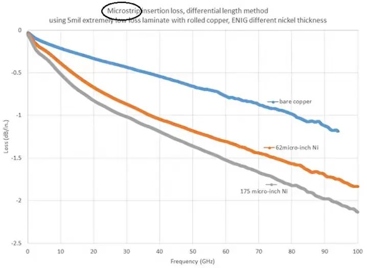
Figure: Insertion Loss of Bare Copper and ENIG-Plated Copper with Two Nickel Thicknesses, Where Thicker ENIG Plating Results in Higher Losses
About Maxipcb
Maxipcb empowers innovators to turn cutting-edge technologies into reality.
We offer one-stop solutions for design, simulation, testing, PCB manufacturing, component procurement and SMT assembly, enabling efficient development, rapid deployment and risk control across the full product lifecycle.Serving the world in communications, industrial automation, aerospace, automotive, semiconductor and beyond, we build a safer, more connected future together.
