Stack-up structure is a critical factor affecting the EMC performance of PCBs and an important method to suppress electromagnetic interference. With the continuous emergence of high-speed circuits, the complexity of PCBs is increasing. To avoid interference from electrical factors, signal layers and power layers must be separated, which involves the stack-up design of HDI PCBs. So what are the common stack-up structures of HDI PCBs?
Stack-up structure is a critical factor affecting the EMC performance of PCBs and an important method to suppress electromagnetic interference. With the continuous emergence of high-speed circuits, the complexity of PCBs is increasing. To avoid interference from electrical factors, signal layers and power layers must be separated, which involves the stack-up design of HDI PCBs. So what are the common stack-up structures of HDI PCBs?
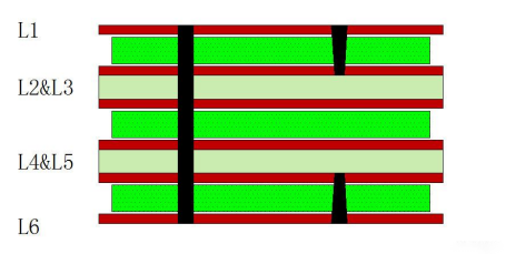
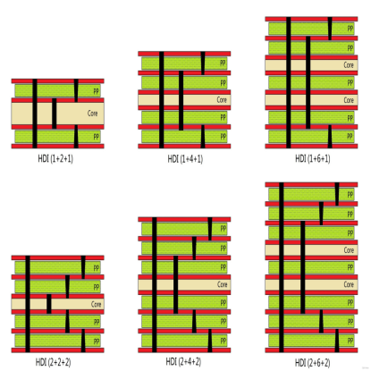
1. Simple Single Build-Up Printed Circuit Board (6-layer single build-up board, stack-up structure: 1+4+1)
This type of board is the simplest, with no buried vias in the inner multilayer board, and can be completed by one-time lamination. Although it is a single build-up board, its manufacturing process is very similar to that of conventional multilayer boards with one-time lamination. The only difference from conventional multilayer boards in the subsequent process is that multiple processes such as laser drilling of blind vias are required. Since there are no buried vias in this stack-up structure, during manufacturing, Layer 2 and Layer 3 can be made into one core board, Layer 4 and Layer 5 into another core board, dielectric layers and copper foils are added to the outer layers, and dielectric layers are added in the middle for one-time lamination. It is very simple and has a lower cost than conventional single build-up boards.
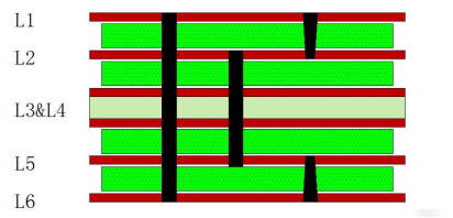
2. Conventional Single Build-Up HDI Printed Circuit Board (6-layer single build-up HDI board, stack-up structure: 1+4+1)
This type of board adopts the (1+N+1) structure (N≥2, N is an even number), which is the mainstream design of single build-up boards in the industry at present. The inner multilayer board has buried vias and requires two-time lamination. This type of single build-up board has not only blind vias but also buried vias. If designers can convert this type of HDI board into the simple single build-up board in Type 1 above, it will be beneficial to both suppliers and demanders.
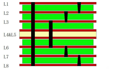
3. Conventional Double Build-Up HDI Printed Circuit Board (8-layer double build-up HDI board, stack-up structure: 1+1+4+1+1)
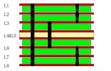
This type of board adopts the (1+1+N+1+1) structure (N≥2, N is an even number), which is the mainstream design of double build-up boards in the industry at present. The inner multilayer board has buried vias and requires three-time lamination. It is mainly designed without stacked vias, and the manufacturing difficulty is normal. If the buried vias of Layers 3-6 are optimized to the buried vias of Layers 2-7 as mentioned above, one-time lamination can be reduced, the process is optimized, and the cost is reduced. This type is shown in the following example.
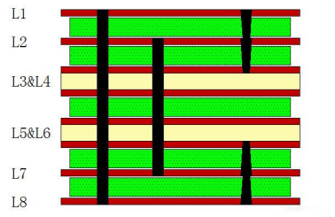
4. Another Conventional Double Build-Up HDI Printed Circuit Board (8-layer double build-up HDI board, stack-up structure: 1+1+4+1+1)
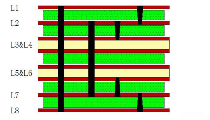
This type of board adopts the (1+1+N+1+1) structure (N≥2, N is an even number). Although it is a double build-up structure, the buried vias are located between Layers 2-7 instead of Layers 3-6. This design can also reduce one-time lamination, optimizing the three-time lamination process of double build-up HDI boards to two-time lamination. However, this type of board has another manufacturing difficulty: the blind vias of Layers 1-3 need to be split into blind vias of Layers 1-2 and Layers 2-3, which requires the inner blind vias of Layers 2-3 to be manufactured with via-filling technology. That is to say, the inner blind vias of double build-up are manufactured with via-filling technology. Generally, the cost of HDI boards with via-filling technology is higher than those without, and the manufacturing difficulty is significantly greater. Therefore, for conventional double build-up boards, it is recommended to avoid stacked via design as much as possible during the design process, and convert the Layers 1-3 blind vias into staggered Layers 1-2 blind vias and Layers 2-3 buried (blind) vias. Experienced designers can adopt this simplified design optimization to reduce the manufacturing cost of their products.
5. Another Unconventional Double Build-Up HDI Printed Circuit Board (6-layer double build-up HDI board, stack-up structure: 1+1+2+1+1)
This type of board adopts the (1+1+N+1+1) structure (N≥2, N is an even number). Although it is a double build-up structure, it also has cross-layer blind vias, and the depth capacity of the blind vias is significantly increased. The depth of the Layers 1-3 blind vias is double that of conventional Layers 1-2 blind vias. Customers with this design have unique requirements and do not allow the cross-layer blind vias of Layers 1-3 to be made into stacked blind vias (Layers 1-2, Layers 2-3). In addition to the difficulty of laser drilling, the subsequent copper deposition (PTH) and electroplating of cross-layer blind vias are also major difficulties. Generally, PCB manufacturers without certain technical capabilities can hardly manufacture this type of board, and the manufacturing difficulty is significantly higher than that of conventional double build-up boards. This design is not recommended unless there are special requirements.
6. Double Build-Up HDI with Stacked Blind Via Design, with Blind Vias Stacked Above Buried Vias (Layers 2-7) (8-layer double build-up HDI board, stack-up structure: 1+1+4+1+1)
This type of board adopts the (1+1+N+1+1) structure (N≥2, N is an even number). This structure is used in some double build-up boards in the industry at present. The inner multilayer board has buried vias and requires two-time lamination. It is mainly designed with stacked vias instead of the cross-layer blind via design in Type 5 above. The main feature of this design is that blind vias need to be stacked above the buried vias of Layers 2-7, which increases the manufacturing difficulty. The buried vias designed in Layers 2-7 can reduce one-time lamination, optimize the process, and reduce the cost.
7. Double Build-Up HDI with Cross-Layer Blind Via Design (8-layer double build-up HDI board, stack-up structure: 1+1+4+1+1)
This type of board adopts the (1+1+N+1+1) structure (N≥2, N is an even number). This structure is a double build-up board with certain manufacturing difficulties in the industry at present. With this design, the inner multilayer board has buried vias in Layers 3-6 and requires three-time lamination. It is mainly designed with cross-layer blind vias, and the manufacturing difficulty is high. HDI PCB manufacturers without certain technical capabilities can hardly manufacture this type of double build-up board. If the cross-layer blind vias of Layers 1-3 are optimized and split into Layers 1-2 and Layers 2-3 blind vias, this split method of staggered vias (not the stacked via split method in Type 4 and Type 6 above) will greatly reduce the manufacturing cost and optimize the production process.
8. Optimization of HDI Boards with Other Stack-Up Structures
For triple build-up printed circuit boards or PCBs with more than three build-up layers, optimization can also be carried out in accordance with the design concept provided above. A complete triple build-up HDI board requires four-time lamination in the entire production process. If the design idea similar to the single build-up board or double build-up board above is considered, one-time lamination process can be completely reduced, thereby improving the finished product rate of the board. Among our many customers, there are many such examples. The initially designed stack-up structure required four-time lamination, but after the optimization of the stack-up structure design, the PCB production only needs three-time lamination to meet the functional requirements of the triple build-up board.
Common HDI Stack-Up Structures
About Maxipcb
Maxipcb empowers innovators to turn cutting-edge technologies into reality.
We offer one-stop solutions for design, simulation, testing, PCB manufacturing, component procurement and SMT assembly, enabling efficient development, rapid deployment and risk control across the full product lifecycle.Serving the world in communications, industrial automation, aerospace, automotive, semiconductor and beyond, we build a safer, more connected future together.