With the continuous increase of communication speed in electronic systems, signal integrity issues in the interconnection area between BGA packages and PCBs have become increasingly prominent.
This paper conducts design and optimization for high-speed differential interconnection structures of BGA packages and PCBs. It mainly analyzes the specific impacts of four key factors on the transmission performance and crosstalk of high-speed differential signals, including differential routing schemes, signal layout schemes, signal-to-ground via ratio, routing layers and via stubs.
A 3D simulation model is established by adopting the full-wave electromagnetic field simulation software CST. Time-domain and frequency-domain simulation results verify that the proposed optimization methods can effectively improve the transmission performance of high-speed differential signals, reduce crosstalk between signals and achieve superior signal isolation.
In recent years, Ball Grid Array (BGA) packages have been widely adopted for high-speed ICs due to their advantages such as compact size, abundant pins, excellent signal integrity and good heat dissipation performance.
To adapt to high-speed signal transmission, differential signaling has become a mainstream solution for chips. As the number of I/O pins on chips keeps growing and the pitch of BGA solder joints continues to shrink, the parasitic effects generated by differential interconnection structures composed of solder joints, vias and traces will trigger a series of signal integrity problems including attenuation and crosstalk, which poses severe challenges to high-speed interconnection design.
Currently, most domestic and overseas researches on board-level signal integrity focus on the modeling and simulation of horizontal transmission lines or individual vias, with the operating frequency generally limited within 20 GHz. There are relatively few studies on the transmission performance and coupling characteristics of differential interconnection structures integrating vias and transmission lines, and limited technical solutions are available to mitigate crosstalk between vertical vias in the package-to-PCB interconnection region.
This paper targets the design and optimization of high-speed BGA package and PCB differential interconnection structures. It elaborates on how four improvement measures — optimized differential routing schemes, revised signal layout schemes, adjusted signal-to-ground via ratio, and improved routing layers plus backdrilling — enhance the transmission performance of high-speed differential signals and suppress crosstalk. A 3D physical model is built using CST Microwave Studio, a full-wave electromagnetic field simulation tool. The simulation frequency reaches 40 GHz, and the effectiveness of the proposed optimization methods is validated in both time domain and frequency domain.
1 Physical Model
1.1 Differential Interconnection Structure
In high-speed signal transmission systems, differential signals are widely applied owing to their capabilities of mitigating rail collapse and electromagnetic interference (EMI), boosting gain, and eliminating interference from common-mode noise and switching noise. High-speed differential signals propagate to each layer of the PCB through the IC package. To realize electrical connection between the BGA package substrate and all PCB layers, the differential interconnection structure is formed by horizontal differential traces and vertical differential vias.
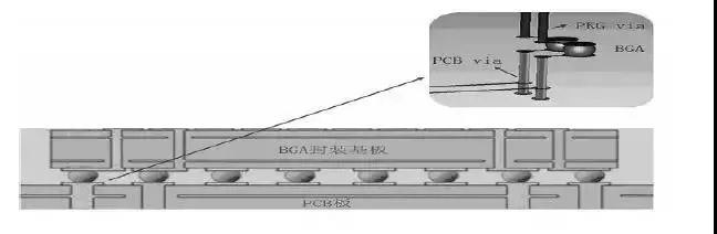 Figure 1 Vertical interconnection structure between BGA package and PCB
1.2 Simulation Environment and Parameter Settings
All simulations in this work are carried out on CST Microwave Studio, a full-wave electromagnetic field simulation software. This platform integrates time-domain and frequency-domain algorithms as well as multiple full-wave and high-frequency algorithms. It supports S-parameter simulation for structures made of arbitrary materials with any configurations, and can also perform co-simulation with circuit design software.
All optimized schemes are modeled as 3D physical structures in CST Microwave Studio. The PCB stack-up structure is shown in Figure 2. The PCB consists of 12 layers in total: Layer 1, Layer 3, Layer 5, Layer 8, Layer 10 and Layer 12 are signal routing layers, while Layer 2, Layer 4, Layer 6, Layer 7, Layer 9 and Layer 11 serve as power or ground planes. The overall board thickness is 97.6 mil, the dielectric constant of the PCB material is 3.8, and the loss tangent is 0.012.
For BGA with a pitch of 0.8 mm, the pitch of fan-out vias is 31.4 mil, the via diameter is 8 mil, and the trace width and trace spacing are both 5 mil. Differential traces are arranged on Layer 10.
 Figure 2 Cross-section of PCB stack-up structure
2 Design and Optimization
Four aspects are optimized to improve the transmission performance of high-speed differential signals and suppress inter-signal crosstalk, namely differential routing schemes, signal layout schemes, signal-to-ground via ratio, as well as routing layer selection and via stubs. All simulation results are presented in the form of S-parameters with a maximum frequency of 40 GHz, and the effectiveness of the optimization methods is verified in both time domain and frequency domain.
2.1 Routing Scheme
When differential signals are led out from vias, different routing schemes exert significant impacts on the transmission characteristics of differential signals. Mismatched length and spacing of transmission lines will cause signal distortion and introduce common-mode noise.
As illustrated in Figure 3, three routing schemes are adopted for traces led out from vias: 0° bend, 90° bend and 45° bend. Two isolated ground vias are placed around each pair of differential vias, and all traces are routed on Layer 10 of the PCB.
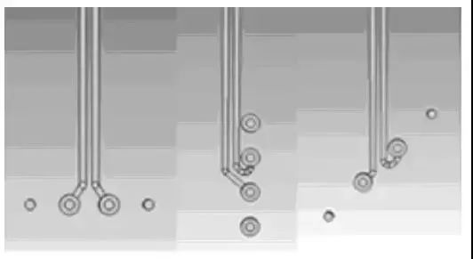 Figure 3 Three routing schemes for differential trace lead-out
Figure 4 shows the insertion loss curves corresponding to the three routing schemes. Apparently, the horizontally symmetric 0° routing scheme delivers the optimal transmission performance. Length and spacing matching are critical for differential signals. Uniform trace length ensures accurate timing and signal symmetry. Any time delay deviation or misalignment between the two traces of a differential pair will distort differential signals, convert part of differential signals into common-mode signals and further induce electromagnetic interference.
Uniform trace spacing maintains consistent differential impedance. Neither 45° bend nor 90° bend routing can achieve ideal length and spacing matching, which will result in phase deviation and common-mode noise.
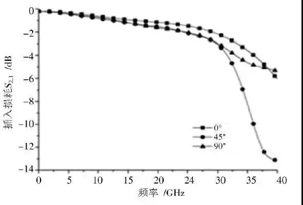 Figure 4 Insertion loss of differential pairs under different routing schemes
Figure 5 and Figure 6 present the common-mode noise generated by the three routing schemes in frequency domain and time domain respectively. Both 45° bend and 90° bend routing produce much higher common-mode noise compared with 0° routing, and the performance of 45° bend routing is slightly better than that of 90° bend routing.
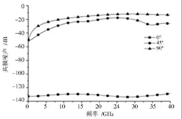 Figure 5 Frequency-domain comparison of common-mode noise under different routing schemes
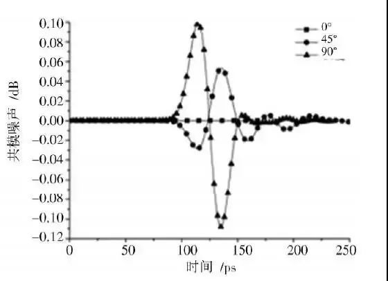 Figure 6 Time-domain comparison of common-mode noise under different routing schemes
According to empirical rules, to limit trace misalignment within 10% of the signal rise edge, the length deviation between the two traces shall be controlled within 10% of the spatial extension of the rise edge. The required length matching tolerance for total trace length is calculated as follows:
ΔL =0.1×RT×v
Where: \(\Delta L\) refers to the maximum allowable length deviation between two traces to keep misalignment below 10% of the rise edge; RT represents the signal rise edge; v stands for the propagation velocity of differential signals. Given that the signal propagation velocity is approximately 6 in/ns and the rise edge is 100 ps, the length deviation between the two traces shall be less than 60 mil.
As the rise time of high-speed signals continues to decrease, the allowable budget for trace length deviation keeps shrinking, which makes trace length matching increasingly important.
Therefore, the horizontally symmetric 0° routing scheme is highly recommended in practical applications to realize precise length and spacing matching.
2.2 Signal Layout Scheme
BGA pins are fanned out and connected to different PCB layers via vias. When dozens of differential pairs are routed in parallel with high density and long trace length, crosstalk will occur between adjacent transmission lines due to the effects of electric and magnetic fields (coupling capacitance and coupling inductance). Signals transmitted on one differential pair will interfere with neighboring traces.
Since the arrangement of BGA solder joints is fixed, the positions of pads and vias are determined by the solder joint layout. Reasonable layout of BGA pins can effectively reduce crosstalk between differential pairs. Two different signal layout schemes are shown in Figure 7.
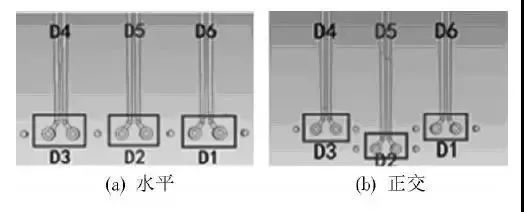 Figure 7 Different signal layout schemes
Two layout configurations are studied: three differential pairs arranged horizontally in parallel, and three differential pairs arranged orthogonally. Two isolated ground vias are deployed around each differential pair. The middle differential pair is set as the victim line, and the two pairs on both sides act as aggressor lines. The three differential pairs are defined as six differential ports (D1 to D3 for BGA fan-out ports). The far-end crosstalk from port D4 and port D6 to port D2 is analyzed to evaluate crosstalk between adjacent channels. Due to bilateral symmetry, only the crosstalk from port D4 to port D2 is discussed. The comparison of far-end crosstalk of differential pairs is shown in Figure 8.
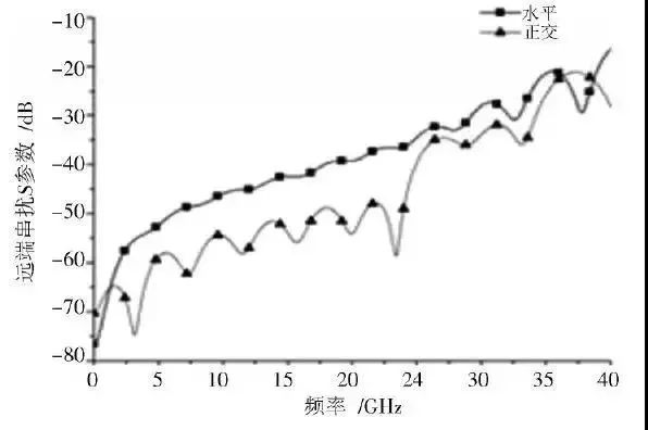 Figure 8 Comparison of far-end crosstalk of differential pairs under different signal layout schemes
As shown in Figure 8, the orthogonal layout increases the spacing between vias and weakens via-to-via coupling. Consequently, the far-end crosstalk from port D4 to port D2 is lower than that under the horizontal layout.
As listed in Table 1, the optimized orthogonal layout reduces far-end crosstalk by 5~15 dB in the frequency band above 5 GHz compared with the original horizontal layout. The superiority of orthogonal layout is also verified by time-domain results in Figure 9. The peak transient noise of the optimized design is reduced by 10 mV, as recorded in Table 1.
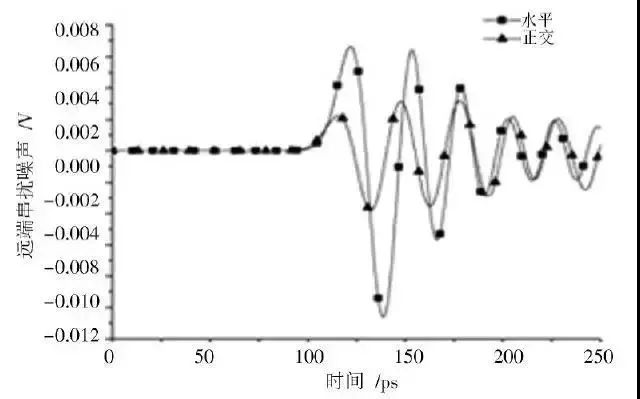 Figure 9 Time-domain response comparison of far-end crosstalk of differential pairs under different signal layout schemes
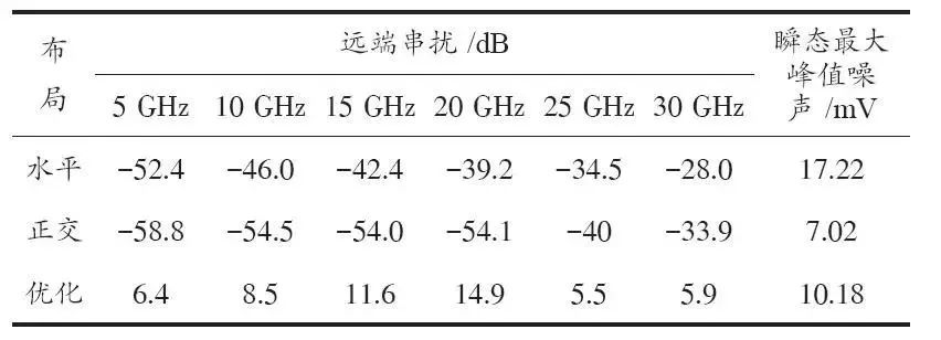 Table 1 Comparison of far-end crosstalk
2.3 Signal-to-Ground Via Ratio
The pitch of BGA solder joints is fixed in practical design, so it is impractical to simply increase the spacing between signal vias to suppress crosstalk. A cost-effective solution is to add surrounding ground vias for isolation around critical signal vias.
Four schemes with signal-to-ground (S/G) via ratios of 1:1, 1:2, 1:3 and 1:4 are adopted in this section. All signal layouts follow the orthogonal configuration proposed in Section 2.2, as shown in Figure 10.
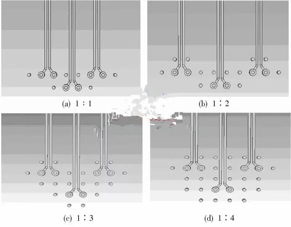 Figure 10 Signal layouts with different signal-to-ground via ratios
Figure 11 compares the far-end crosstalk of the four schemes. The scheme with an S/G ratio of 1:2 achieves a remarkable reduction in far-end crosstalk compared with the 1:1 ratio scheme. According to Table 2, within the frequency range of 5~30 GHz, the far-end crosstalk is decreased by 8~17 dB when the S/G ratio changes from 1:1 to 1:2.
Adding ground vias around signal vias shortens the ground return path and mitigates inductive discontinuity of signal vias, thereby suppressing crosstalk to a certain extent. However, the optimization effect tends to saturate quickly. There is only a marginal difference between the 1:3 and 1:4 S/G ratio schemes, with limited further improvement in far-end crosstalk.
The time-domain simulation results of far-end crosstalk for the four schemes are presented in Figure 12, which draw the same conclusion as frequency-domain analysis. The peak transient noise of each scheme is extracted from time-domain waveforms: the peak noise reaches 22 mV at the S/G ratio of 1:1, drops sharply to 6 mV at 1:2, and stabilizes at approximately 1.6 mV for both 1:3 and 1:4 (a difference less than 0.03 mV). The detailed data are summarized in Table 2.
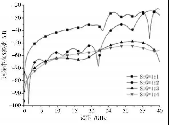 Figure 11 Comparison of far-end crosstalk of four schemes
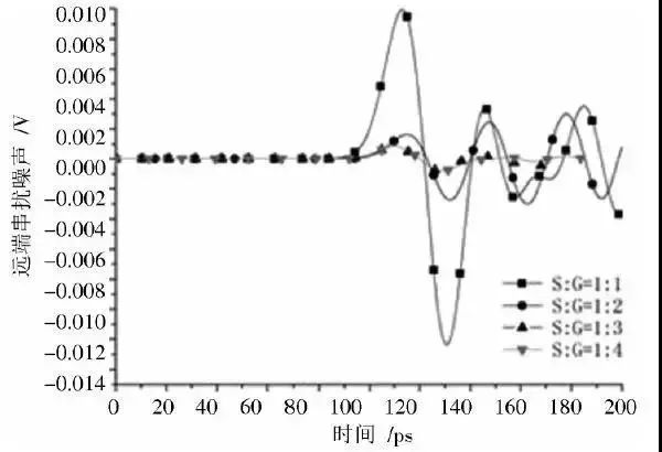 Figure 12 Time-domain response comparison of far-end crosstalk of four schemes
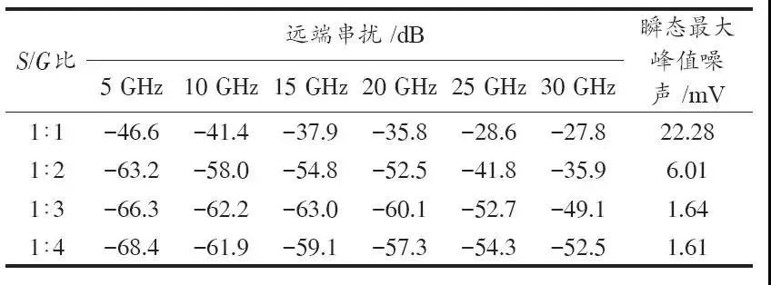 Table 2 Comparison of far-end crosstalk
The total number of BGA pins is limited, so ground vias cannot be increased without restriction. Balancing crosstalk performance and pin resource utilization, the 1:2 S/G ratio is sufficient for applications below 20 GHz, as its performance is comparable to the 1:3 ratio. For operating frequencies above 20 GHz, the 1:3 S/G ratio outperforms the 1:2 ratio obviously.
2.4 Influence of Routing Layer Selection and Via Stubs
Adding ground vias for isolation is a simple method to reduce crosstalk, yet its optimization effect will soon reach saturation and fail to provide ideal shielding performance.
In the interconnection region between packages and PCBs, both via coupling and trace coupling between high-speed differential pairs are major sources of crosstalk. On the basis of the above three optimization directions, this section further analyzes the impacts of routing layers and via stubs on crosstalk.
Four configurations are designed as shown in Figure 13, where three differential pairs are placed on different layers with varying via stub lengths. All signals adopt the orthogonal layout, and six isolated ground vias are arranged around each differential via pair.
- Configuration (a): All three differential pairs are routed on PCB Layer 10 near the bottom layer.
- Configuration (b): The two aggressor differential pairs on both sides are moved from Layer 10 to Layer 3, and the long via stubs are removed via 59.1 mil backdrilling. This design greatly shortens the vertical length of via coupling between the aggressor signals on both sides and the victim signal in the middle.
- Configuration (c): Opposite to Configuration (b), the middle victim differential pair is routed on Layer 3 with backdrilling, while the two aggressor pairs on both sides are placed on Layer 10.
- Configuration (d): The middle victim differential pair is routed on Layer 10, the two aggressor pairs are placed on Layer 3, and the long via stubs are retained.
The frequency-domain comparison of far-end crosstalk is shown in Figure 14. Compared with Configuration (a), Configuration (b) shortens the vertical length of aggressor signal vias and reduces via coupling. Meanwhile, the three differential pairs are placed on different layers, which weakens trace-to-trace coupling and achieves a significant crosstalk reduction.
As shown in Table 3, within the 5~30 GHz frequency band, Configuration (b) reduces far-end crosstalk by 4~12 dB compared with Configuration (a). Configuration (c) introduces extra via-trace coupling: although via coupling is reduced by placing the victim line on Layer 3 with backdrilling, the long vias of the two aggressor pairs will generate severe trace interference on the middle differential pair.
In Configuration (b), the aggressor vias are processed with backdrilling, so no long stubs will interfere with the victim differential signals during signal transmission. Therefore, Configuration (b) delivers the optimal crosstalk performance. Without backdrilling (Configuration d), even if differential pairs are arranged on different layers, the long via stubs will damage impedance continuity, cause resonance of local differential signals, and aggravate crosstalk between adjacent differential pairs. Its performance is even inferior to Configuration (a) where all signals are routed near the bottom layer.
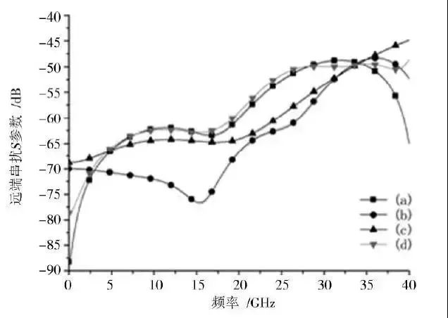 Figure 14 Comparison of far-end crosstalk of four schemes
Time-domain simulation results are consistent with frequency-domain analysis, as shown in Figure 15. Table 3 lists the peak transient noise of all four configurations, where Configuration (b) has the lowest noise level and Configuration (d) has the highest.
In practical design, to avoid interference caused by long via stubs, differential traces are recommended to be routed near the PCB bottom layer and designed as internal striplines. For multiple parallel differential pairs, distributing them on different signal layers can suppress crosstalk. In particular, backdrilling must be applied to vias of signals routed on upper PCB layers.
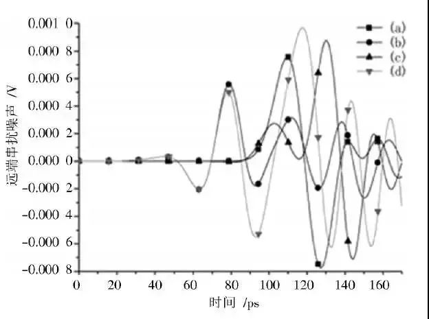 Figure 15 Time-domain response comparison of far-end crosstalk of four schemes
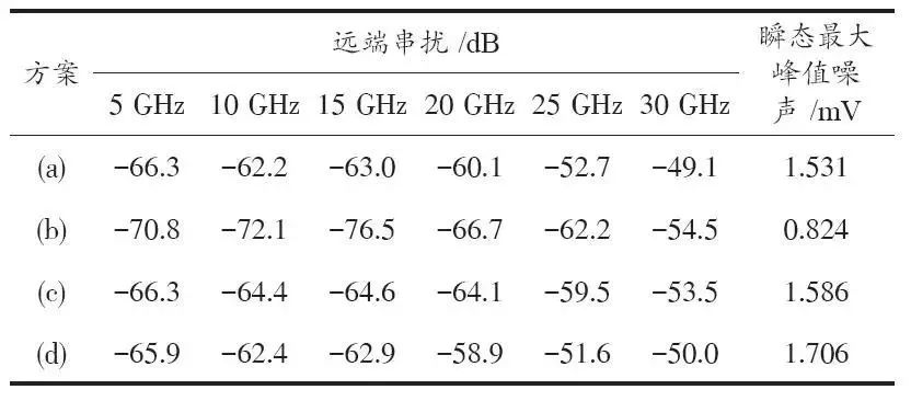 Table 3 Comparison of far-end crosstalk
3 Comparison and Analysis of Simulation Results
Based on the comparison and analysis of the above simulation data, the following design and optimization guidelines are summarized:
- When leading differential signals out from vias, adopt horizontally symmetric routing to realize precise length and spacing matching, so as to obtain optimal transmission performance and minimum common-mode noise. If full horizontal symmetry cannot be achieved in layout, 45° bend routing is preferred over 90° bend routing.
- Orthogonal layout of BGA pins can effectively suppress crosstalk between differential pairs. Compared with horizontal layout, orthogonal layout reduces crosstalk by 5~15 dB in the 5~30 GHz frequency range.
- Deploying ground vias around critical signal vias can mitigate crosstalk, while the optimization effect will gradually saturate. For operating frequencies below 20 GHz, placing four ground vias around each signal pair can effectively suppress crosstalk and meet signal integrity requirements. For frequencies above 20 GHz, six isolated ground vias are suggested around high-speed signal vias for further crosstalk reduction.
- In terms of routing layer selection, route differential traces near the PCB bottom layer and adopt internal stripline structures to eliminate interference from long via stubs. For multiple parallel differential pairs, distribute them on different signal layers to reduce crosstalk, and ensure backdrilling is implemented for vias of signals on upper layers.
4 Conclusion
This paper carries out optimal design for high-speed differential interconnection structures between BGA packages and PCBs. A 3D simulation model is established based on CST full-wave electromagnetic field simulation software. The influences of four key factors — differential routing schemes, signal layout schemes, signal-to-ground via ratio, routing layers and via stubs — on the transmission performance and crosstalk of high-speed differential signals are systematically studied.
Time-domain and frequency-domain simulation results prove that the proposed optimization methods can effectively improve the transmission performance of high-speed differential signals, reduce inter-pair crosstalk and enhance signal isolation.
The research results provide a valuable reference for ensuring signal integrity of high-speed signal transmission systems and offer practical guidance for high-speed PCB design.
About Maxipcb
Maxipcb empowers innovators to turn cutting-edge technologies into reality.
We offer one-stop solutions for design, simulation, testing, PCB manufacturing, component procurement and SMT assembly, enabling efficient development, rapid deployment and risk control across the full product lifecycle.Serving the world in communications, industrial automation, aerospace, automotive, semiconductor and beyond, we build a safer, more connected future together.
