PCB (Printed Circuit Board) is a critical electronic component that serves as the support structure for electronic components. Manufactured using electronic printing technology, it is known as a "printed" circuit board.
PCB (Printed Circuit Board) is a critical electronic component that serves as the support structure for electronic components. Manufactured using electronic printing technology, it is known as a "printed" circuit board.
Before the advent of PCBs, circuits were constructed using point-to-point wiring. This method offered low reliability, as wire breakage due to aging caused open circuits or short circuits at connection nodes. Wire-wrapping technology represented a major advancement in circuit engineering; by winding small-gauge wires around posts at connection points, it improved circuit durability and replaceability.
As the electronics industry evolved from vacuum tubes and relays to silicon semiconductors and integrated circuits, the size and cost of electronic components decreased. Electronic products became increasingly prevalent in consumer applications, driving manufacturers to seek smaller, more cost-effective solutions. Thus, the PCB was invented.
PCB Manufacturing Process
The production of PCBs is highly complex. Taking a 4-layer printed circuit board as an example, the manufacturing process mainly includes PCB layout verification, core board fabrication, inner-layer pattern transfer, core board drilling and inspection, lamination, drilling, electroless copper deposition on hole walls, outer-layer pattern transfer, and outer-layer etching.
1. PCB Layout
The first step in PCB manufacturing is to organize and inspect the PCB layout. Upon receiving CAD files from PCB design companies, PCB manufacturers convert the files into a unified format—Extended Gerber RS-274X or Gerber X2—since each CAD software uses a unique file format. Engineers at the factory then inspect the PCB layout for compliance with manufacturing processes and any defects.
2. Core Board Fabrication
The copper-clad laminate (CCL) is cleaned; dust contamination can cause short circuits or open circuits in the final circuit.
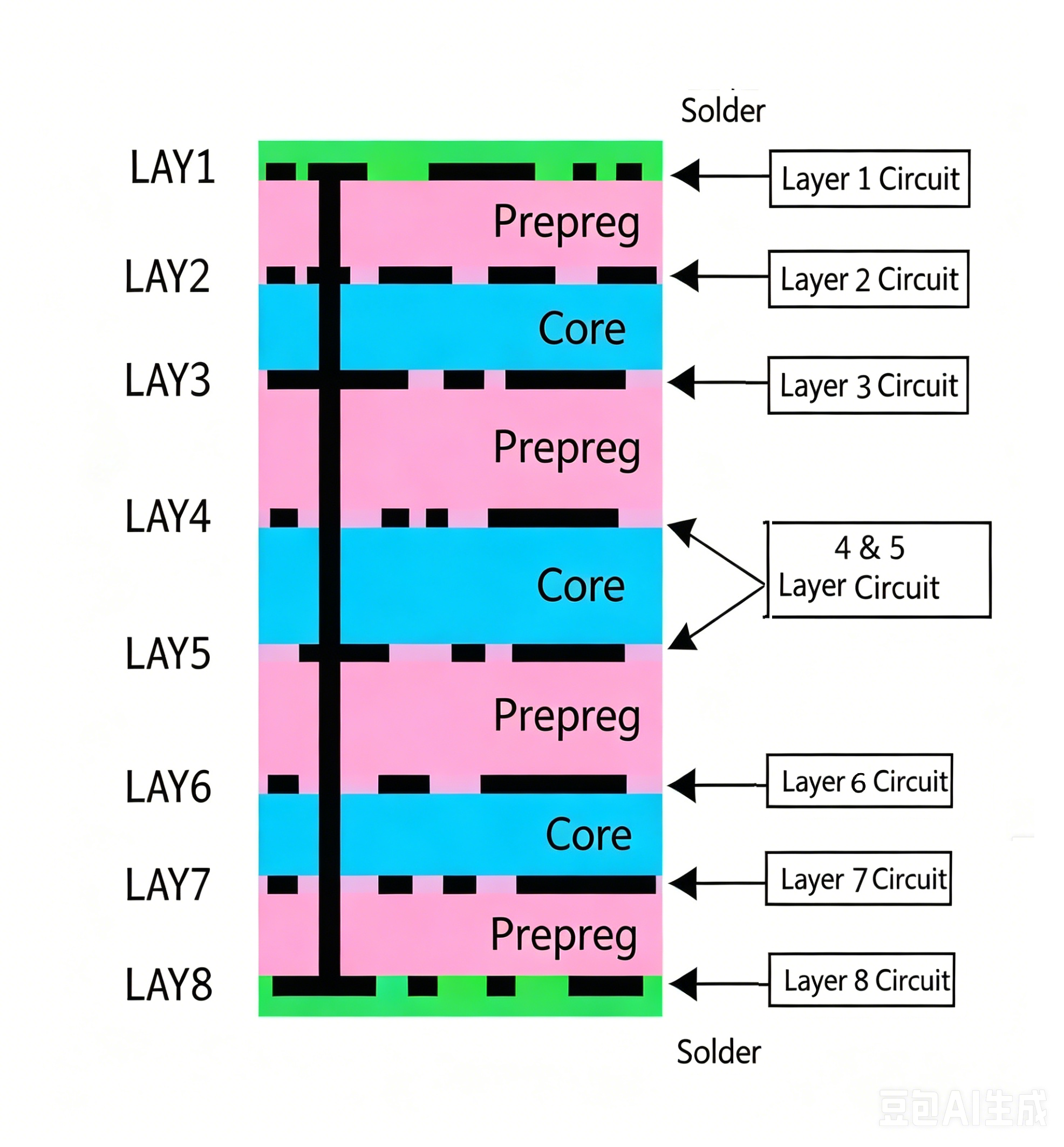
The diagram below shows an 8-layer PCB, which is actually assembled from 3 copper-clad laminates (core boards) and 2 copper foils, bonded together with prepreg. Fabrication starts from the innermost core board (Layers 4 and 5), with layers sequentially stacked and secured. The fabrication of a 4-layer PCB follows a similar process, using 1 core board and 2 copper foils.
3. Inner-Layer PCB Pattern Transfer
First, the two-layer circuit pattern is fabricated on the innermost core board. After cleaning, a layer of photoresist film is applied to the surface of the copper-clad laminate. This film cures upon exposure to light, forming a protective layer on the copper foil of the CCL.
The two-layer PCB layout films are aligned with the double-sided CCL, with the top PCB layout film inserted to ensure precise stacking alignment.
A UV exposure unit irradiates the photoresist film on the copper foil. The photoresist under the transparent areas of the film cures, while the photoresist under opaque areas remains uncured. The copper foil covered by the cured photoresist forms the desired PCB circuit pattern, functioning similarly to the toner of a laser printer in manual PCB fabrication.
Uncured photoresist is removed using an alkaline solution, leaving the required copper circuit pattern protected by the cured photoresist.
Unwanted copper foil is then etched away using a strong alkaline solution such as NaOH.
The cured photoresist is stripped, revealing the desired PCB circuit copper pattern.
4. Core Board Drilling and Inspection
The core board is now complete. Alignment holes are drilled in the core board to facilitate alignment with other materials in subsequent steps.
Once the core board is laminated with other PCB layers, modifications are impossible, making inspection critical. Automated optical inspection (AOI) machines compare the core board against the PCB layout drawings to detect errors.
5. Lamination
A new material, prepreg (B-stage resin), is used as an adhesive between core boards (for PCBs with >4 layers) and between core boards and outer-layer copper foils, while also providing electrical insulation.
The bottom copper foil and two layers of prepreg are pre-aligned and secured to the bottom steel plate via alignment holes. The fabricated core board is placed over the alignment holes, followed by sequential stacking of two prepreg layers, one copper foil layer, and one pressure-bearing aluminum plate.
The PCB assemblies clamped between steel plates are placed on a rack and fed into a vacuum hot press for lamination. High temperatures melt the epoxy resin in the prepreg, bonding the core boards and copper foils together under pressure.
After lamination, the top steel plate is removed, followed by the pressure-bearing aluminum plate (which also isolates PCBs and ensures smooth outer-layer copper foils). The resulting PCB is covered with smooth copper foil on both sides.
6. Drilling
To connect the four isolated copper layers within the PCB, through-holes are drilled through the entire board, followed by metallization of the hole walls for electrical conductivity.
An X-ray drilling machine locates and aligns the inner core board, automatically positioning the hole locations and drilling pilot holes to ensure central alignment during subsequent drilling.
An aluminum plate is placed on the drilling machine bed, followed by the PCB. For efficiency, 1–3 identical PCBs are stacked and drilled based on layer count. Finally, an aluminum plate is placed on top of the uppermost PCB; the top and bottom aluminum plates prevent copper foil tearing when the drill bit enters and exits the PCB.
Excess epoxy resin squeezed out during lamination is removed. A profile milling machine cuts the PCB perimeter to the correct XY coordinates.
7. Electroless Copper Deposition on Hole Walls
Nearly all PCB designs use through-holes to connect circuits on different layers. A reliable connection requires a 25μm copper film on the hole walls. This thickness is achieved via electroplating, but the hole walls consist of non-conductive epoxy resin and fiberglass.
First, a conductive layer is deposited on the hole walls. Electroless copper deposition forms a 1μm copper film across the entire PCB surface, including the hole walls. The entire process—chemical treatment, cleaning, etc.—is machine-controlled.
8. Outer-Layer PCB Pattern Transfer
Next, the outer-layer PCB pattern is transferred to the copper foil. The process follows the same principle as inner-layer pattern transfer, using photographic films and photoresist to transfer the pattern, with the only difference being the use of positive-image processing.
Inner-layer pattern transfer uses the subtractive method with negative-image processing: copper covered by cured photoresist forms the circuit; uncured photoresist is removed, and exposed copper is etched away, leaving the circuit protected by cured photoresist.
Outer-layer pattern transfer uses the additive method with positive-image processing: areas covered by cured photoresist are non-circuit regions. After removing uncured photoresist, electroplating is performed: no plating occurs under the photoresist, while exposed areas are plated with copper followed by tin. After resist stripping, alkaline etching is performed, followed by tin stripping. The circuit pattern remains protected by tin.
The PCB is clamped, and copper is electroplated. As noted, a 25μm copper film on the hole walls is required for sufficient conductivity, with the entire system computer-controlled to ensure precision.
9. Outer-Layer PCB Etching
An automated assembly line performs the etching process. First, the cured photoresist is stripped from the PCB. Unwanted copper foil covered by the resist is etched away using a strong alkaline solution. Tin plating on the PCB circuit copper is removed using a tin stripper. After cleaning, the 4-layer PCB pattern is complete.
About Maxipcb
Maxipcb empowers innovators to turn cutting-edge technologies into reality.
We offer one-stop solutions for design, simulation, testing, PCB manufacturing, component procurement and SMT assembly, enabling efficient development, rapid deployment and risk control across the full product lifecycle.Serving the world in communications, industrial automation, aerospace, automotive, semiconductor and beyond, we build a safer, more connected future together.