SATA is the abbreviation of serial ATA, namely Serial Advanced Technology Attachment. It is a computer bus, whose main function is to realize data transmission between the motherboard and mass storage devices (such as hard disk drives and optical disc drives).
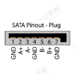
SATA is the abbreviation of serial ATA, namely Serial Advanced Technology Attachment. It is a computer bus, whose main function is to realize data transmission between the motherboard and mass storage devices (such as hard disk drives and optical disc drives). SATA3.0 can provide a theoretical maximum link speed of 6Gbps (750MB/s) between storage units, disk drives, optical and tape drives, and Host Bus Adapters (HBA), which puts forward new design requirements for PCB design. The pin definition of SATA 3.0 is shown in Table 1.
Table 1 Pin Definition of SATA 3.0
| Pin Number |
Signal |
Definition |
| 1 |
GND Ground |
Ground, generally connected to the negative pole |
| 2 |
A+ Transmit |
Positive signal interface for data transmission |
| 3 |
A- Transmit |
Negative signal interface for data transmission |
| 4 |
GND Ground |
Ground, generally connected to the negative pole |
| 5 |
B+ Transmit |
Positive signal interface for data transmission |
| 6 |
B- Transmit |
Negative signal interface for data transmission |
| 7 |
GND Ground |
Ground, generally connected to the negative pole |
1. PCB Design Requirements for SATA3.0
- To prevent signal reflection on the board and overvoltage protection to avoid chip damage, both the transmit and receive AC coupling capacitors of SATA are placed at the connector end, as shown in Figure 1.
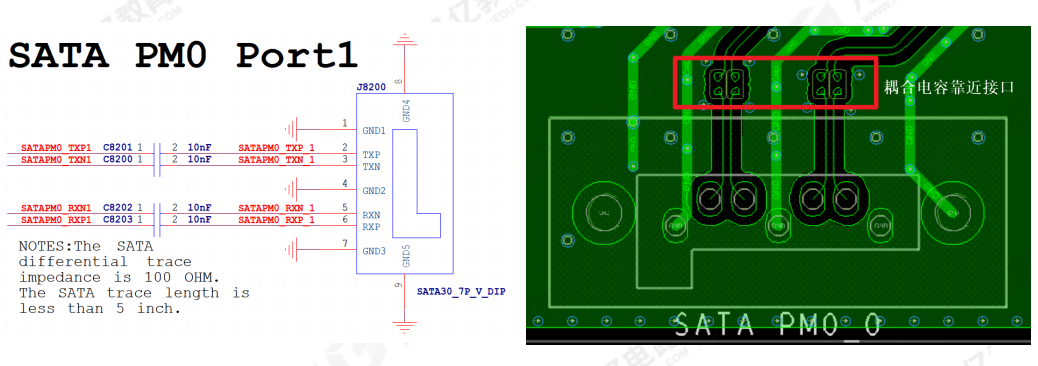
Figure 1 Placement of SATA Coupling Capacitors
- SATA is a high-speed differential signal, including one transmit signal pair and one receive signal pair. It is extremely important to keep the trace length of the differential pair consistent. Mismatched trace length will reduce the difference between the signals, increase the bit error rate, and also generate common-mode noise, thereby increasing EMI radiation. The length mismatch error shall meet the requirement of <6mil, and the intra-pair length matching of the differential pair shall comply with the differential length matching processing specification, as shown in Figure 2.
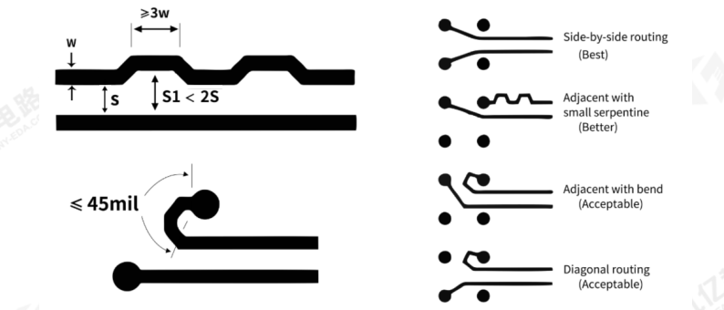
Figure 2 Length Matching Requirements for Differential Routing
-
Differential pairs should be routed on the surface layer of the PCB (microstrip line) as much as possible. If the differential pair must be routed on different layers, the trace length on both sides of the via must be consistent. When changing the routing layer, it is necessary to ensure that there is still a proper return path after the routing layer is changed. The common practice is to add GND vias next to the signal via.
-
A complete reference plane shall be maintained under the differential traces. On both sides of the high-speed traces, the reference plane shall not be cut or have hollowed-out areas within a range of 10 times the height of the trace relative to the reference plane.
The overall requirements are shown in Table 2 below.
Table 2 PCB Routing Requirements for SATA3.0
| Parameter |
Requirement |
| Routing Impedance |
Differential 100ohm±10% (100ohm is recommended preferentially; if 100ohm cannot be achieved through stack-up design, ensure the impedance meets 90ohm±10% at least) |
| Intra-pair Delay Difference of Differential Pair |
<6mil |
| Routing Length |
<6 inches |
| Capacitor Requirement |
10nF±20%, 0201 package recommended |
| Spacing Between Differential Pairs |
Recommended ≥4 times the SATA trace width |
| Spacing Between Differential Signals and Other Signals |
Recommended ≥4 times the SATA trace width |
| Maximum Allowed Number of Vias per Signal |
Recommended no more than 2 |
The PCB routing schematic of SATA3.0 is shown in Figure 3 below.
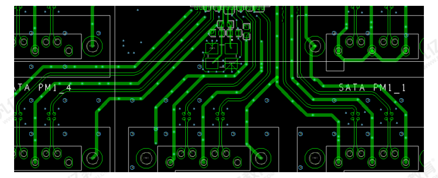
Figure 3 Routing Schematic of SATA Differential Signals
About Maxipcb
Maxipcb empowers innovators to turn cutting-edge technologies into reality.
We offer one-stop solutions for design, simulation, testing, PCB manufacturing, component procurement and SMT assembly, enabling efficient development, rapid deployment and risk control across the full product lifecycle.Serving the world in communications, industrial automation, aerospace, automotive, semiconductor and beyond, we build a safer, more connected future together.