This article constructs a simplified scenario to introduce ground return, power return, and related cross-split issues in high-speed PCBs. For illustration purposes, the layer spacing is exaggerated in the diagrams.
This article constructs a simplified scenario to introduce ground return, power return, and related cross-split issues in high-speed PCBs. For illustration purposes, the layer spacing is exaggerated in the diagrams.
IC1 is the signal output terminal, and IC2 is the signal input terminal (to simplify the PCB model, it is assumed that the receiving end contains an internal pull-down resistor). The third layer is the ground plane. The grounds of both IC1 and IC2 are derived from this ground plane. A power plane is located in the upper right corner of the top layer, connected to the positive power supply. C1 and C2 are the decoupling capacitors for IC1 and IC2, respectively. The power and ground pins shown in the diagram correspond to the power supply and ground for the signal transmitting and receiving terminals.
At low frequencies, if terminal S1 outputs a high level, the entire current loop is: power supply → power plane via conductors → IC1 via the orange path → output from S1 → travel along the layer 2 trace to R1 → enter IC2 → flow into the ground plane → return to the negative power supply via the red path.
However, at high frequencies, the distributed characteristics of the PCB significantly impact signal behavior. The so-called "ground return" is a common issue encountered in high-frequency signals. When the current in the signal line from S1 to R1 increases, the rapidly changing external magnetic field induces a reverse current in nearby conductors. If the third layer is a complete ground plane, a current will flow along the blue dashed line on the ground plane; if the top layer has a complete power plane, a return current will also flow along the blue dashed line on the top layer. At this point, the signal loop has the smallest current loop area, resulting in minimal radiated energy and minimal susceptibility to coupling from external signals (this principle is identical to the skin effect at high frequencies, which also minimizes radiated energy).
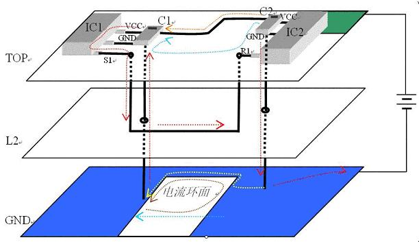
Since high-frequency signals have fast voltage and current changes but short periods, the required energy is not large. Therefore, the chip draws power from the nearest decoupling capacitor. When C1 is sufficiently large and has a fast response time (very low ESR, typically achieved with ceramic capacitors, whose ESR is far lower than tantalum capacitors), the orange path on the top layer and the red path on the ground plane can be considered non-existent (a current corresponding to the entire board power supply exists, but not the current corresponding to the signal shown in the diagram).
Thus, in the constructed environment, the complete current path is: Positive terminal of C1 → VCC pin of IC1 → S1 → Layer 2 signal line → R1 → GND pin of IC2 → Via → Ground plane path → Via → Negative terminal of the capacitor. As can be seen, there is an equivalent brown current in the vertical direction, which induces a magnetic field in the middle. Additionally, this loop area is highly susceptible to coupling from external interference. If the signal in the diagram is a clock signal running parallel to an 8-bit data bus powered by the same power supply from the same chip, the current return path will be identical. If all data lines flip simultaneously in the same direction, a large reverse current will be induced on the clock line. Without proper matching of the clock line, this crosstalk can be fatal to the clock signal.
The intensity of this crosstalk is not proportional to the absolute value of the interference source's high/low level, but to the rate of change of the interference source's current (dI/dt). For a purely resistive load, the crosstalk current is proportional to:
\(dI/dt = dV / (T_{10\%-90\%} \times R)\)
Where dI/dt (current change rate), dV (interference source swing), and R (interference source load) are parameters of the interference source. For capacitive loads, dI/dt is inversely proportional to the square of the rise time (T₁₀%-₉₀%). It follows that low-speed signals do not necessarily produce less crosstalk than high-speed signals. As the saying goes: a 1kHz signal is not necessarily a low-speed signal—its edge characteristics must be considered comprehensively. Signals with steep edges contain many harmonic components with large amplitudes at multiple frequency multiples. Therefore, when selecting devices, avoid blindly choosing chips with excessively fast switching speeds, as this not only increases cost but also exacerbates crosstalk and EMC issues.
Any adjacent power plane or other plane can serve as a return plane for a signal, provided that appropriate capacitors at both ends of the signal provide a low-reactance path to ground. In typical applications, the I/O power supplies of the transmitting and receiving chips are usually the same, and 0.01–0.1μF decoupling capacitors are generally connected between their respective power supplies and ground. These capacitors are precisely located at both ends of the signal, making the power plane's return effect second only to that of the ground plane.
Borrowing other power planes for return, however, often lacks low-reactance paths to ground at both ends of the signal. In such cases, the current induced on the adjacent plane will seek the nearest capacitor to return to ground. If this "nearest capacitor" is far from the start or end of the signal, the return current must travel a long distance to form a complete loop. This shared return path has the same effect as common-ground interference, equivalent to crosstalk between signals.
For unavoidable cross-power-split situations, a high-pass filter composed of a capacitor or an RC series circuit can be connected across the split (e.g., a 10Ω resistor in series with a 680pF capacitor; the specific values depend on the signal type). This provides a high-frequency return path while isolating low-frequency crosstalk between the planes. While adding capacitors between power planes may seem unconventional, it is effective. If prohibited by specifications, capacitors can be connected from each plane to ground at the split location.
When borrowing other planes for return, it is best to add several small capacitors to ground at both ends of the signal to provide a return path. However, this is often difficult to implement, as the surface space near the terminals is usually occupied by matching resistors and chip decoupling capacitors.
About Maxipcb
Maxipcb empowers innovators to turn cutting-edge technologies into reality.
We offer one-stop solutions for design, simulation, testing, PCB manufacturing, component procurement and SMT assembly, enabling efficient development, rapid deployment and risk control across the full product lifecycle.Serving the world in communications, industrial automation, aerospace, automotive, semiconductor and beyond, we build a safer, more connected future together.
