Since RF circuits are distributed-parameter circuits, skin effect and coupling effect are likely to occur during actual circuit operation. Therefore, in actual PCB design, it is often found difficult to control interference radiation in the circuit, such as mutual interference between digital and analog circuits, noise interference from the power supply, and interference caused by unreasonable ground routing.
Since RF circuits are distributed-parameter circuits, skin effect and coupling effect are likely to occur during actual circuit operation. Therefore, in actual PCB design, it is often found difficult to control interference radiation in the circuit, such as mutual interference between digital and analog circuits, noise interference from the power supply, and interference caused by unreasonable ground routing. For this reason, how to weigh the pros and cons and seek an appropriate compromise in the PCB design process to minimize these interferences, or even avoid interference in some circuits, is the key to the success of RF circuit PCB design. This article provides some handling techniques from the perspective of PCB layout, which are of great use in improving the anti-interference capability of RF circuits.
1 RF Layout
What is discussed here is mainly the component placement layout for multilayer boards. The key to component placement layout is to fix the components located on the RF path, adjust their orientation to minimize the length of the RF path, keep the input away from the output, separate high-power circuits and low-power circuits as far as possible, and keep sensitive analog signals away from high-speed digital signals and RF signals.
The following techniques are often used in layout.
1.1 Straight-Line Layout
The components of the main RF signal should be arranged in a straight-line layout as much as possible, as shown in Figure 1. However, due to limitations of the PCB board and cavity space, it is often impossible to arrange them in a straight line. In this case, an L-shaped layout can be used. A U-shaped layout should preferably be avoided (as shown in Figure 2). If it is truly unavoidable, increase the distance between input and output as much as possible, at least 1.5 cm or more.
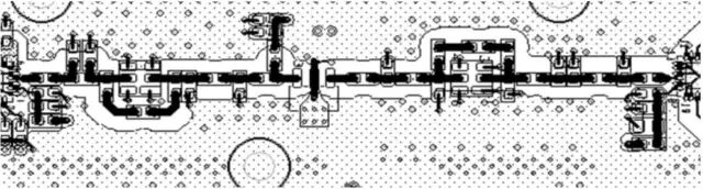
Figure 1 Straight-line layout
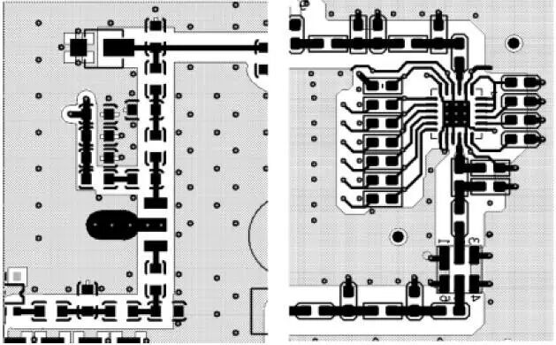
Figure 2 L-shaped and U-shaped layouts
In addition, when using an L-shaped or U-shaped layout, it is best not to turn immediately upon entering the interface, as shown on the left of Figure 3; instead, turn after a short straight section, as shown on the right of Figure 3.
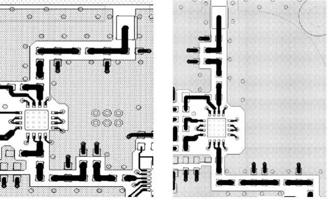
Figure 3 Two schemes
1.2 Identical or Symmetrical Layout
Identical modules should be made into identical layouts or symmetrical layouts as much as possible, as shown in Figures 4 and 5.
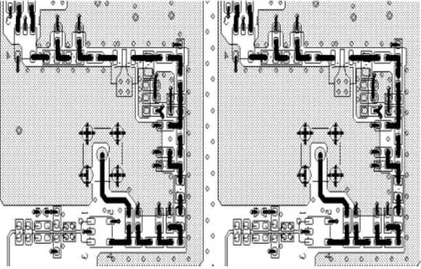
Figure 4 Identical layout
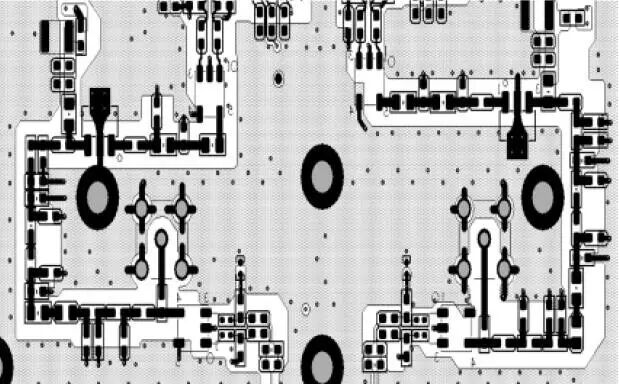
Figure 5 Symmetrical layout
1.3 Cross-Shaped Layout
The feed inductor of the bias circuit should be placed perpendicular to the RF channel, as shown in Figure 6, mainly to avoid mutual inductance between inductive components.
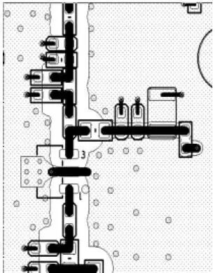
Figure 6 Cross-shaped layout
1.4 45-Degree Layout
To make reasonable use of space, components can be placed at a 45-degree orientation so that the RF line is as short as possible, as shown in Figure 7.
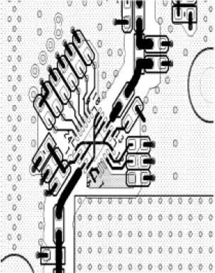
Figure 7 45-degree layout
2 RF Routing
The overall routing requirements are: RF signal traces should be short and straight, minimize abrupt changes in the line, use as few vias as possible, do not intersect with other signal lines, and add as many ground vias as possible around RF signal lines.
The following are some commonly used optimization methods:
2.1 Tapered Line Treatment
When the RF line width is considerably larger than the width of the IC device pins, use a tapered transition for the line width contacting the chip, as shown in Figure 8.
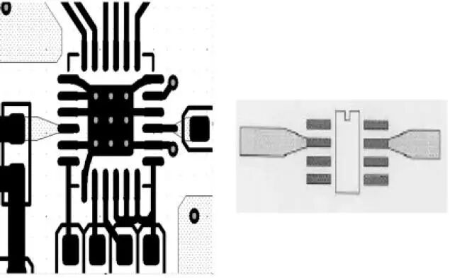
Figure 8 Tapered line
2.2 Arc Line Treatment
When the RF line cannot be straight, use arc routing. This can reduce external radiation from the RF signal and mutual coupling. Experiments have shown that using curved right angles at transmission-line corners can minimize return loss. As shown in Figure 9.
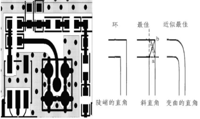
Figure 9 Arc line
2.3 Ground and Power
Ground lines should be as thick as possible. Where conditions permit, pour ground on each layer of the PCB as much as possible, connect the ground to the main ground, add many ground vias, and minimize ground impedance.
For the power supply of RF circuits, plane splitting should be avoided as much as possible. A whole power plane not only increases the radiation of the power plane to RF signals but is also easily interfered with by RF signals. Therefore, power lines or planes are generally made in elongated shapes and handled according to the current. They should be as thick as possible while meeting current-carrying capability, but should not be widened without limit. When handling power lines, be sure to avoid forming loops.
The direction of power and ground lines should be parallel to the direction of the RF signal but must not overlap. Where crossing is necessary, it is best to use perpendicular cross crossings.
2.4 Cross Crossing Treatment
RF signals and IF signal traces should cross each other, and a ground should be placed between them as much as possible.
When RF signals cross other signal traces, place a layer of ground connected to the main ground along the RF trace between them as much as possible. If this is impossible, ensure that they cross perpendicularly. The other signal traces here also include power lines.
2.5 Ground Guarding Treatment
Perform ground guarding on RF signals, interference sources, sensitive signals, and other important signals. This can both improve the anti-interference capability of the signal and reduce interference from that signal to other signals. As shown in Figure 10.
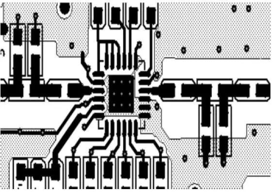
Figure 10 Ground guarding treatment
2.6 Copper Foil Treatment
Copper foil treatment requires smooth and flat shapes; long lines or sharp corners are not allowed. If they cannot be avoided, add several ground vias at sharp corners, thin copper strips, or copper foil edges.
2.7 Spacing Treatment
The RF line must be at least 3W away from the edge of the adjacent ground plane, and there must be no non-grounded vias within the 3W range.
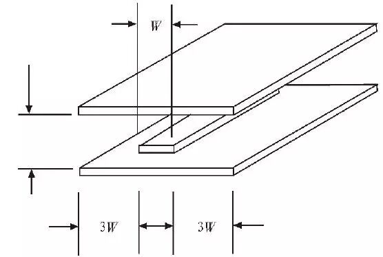
Figure 11 Spacing
RF lines on the same layer should be ground-guarded, and ground vias should be added to the ground copper pour. The via spacing should be less than 1/20 of the wavelength (λ) corresponding to the signal frequency, arranged evenly and neatly. The edge of the ground-guarding copper should be 2W away from the RF line or 3H high, where H represents the total thickness of the adjacent dielectric layers.
3 Cavity Treatment
For the entire RF circuit, RF units of different modules should be isolated with cavities, especially between sensitive circuits and strong radiation sources. In high-power multistage amplifiers, isolation between stages should also be ensured. After the entire circuit branches are properly placed, the shielding cavity is handled. The following points should be noted in shielding cavity treatment:
The entire shielding cavity should be made into a regular shape as much as possible to facilitate molding. Each shielding cavity should be made rectangular as much as possible; avoid square shielding cavities.
The corners of the shielding cavity should use arcs. Shielded metal cavities are generally formed by casting, and arc-shaped corners facilitate draft during casting. As shown in Figure 12.
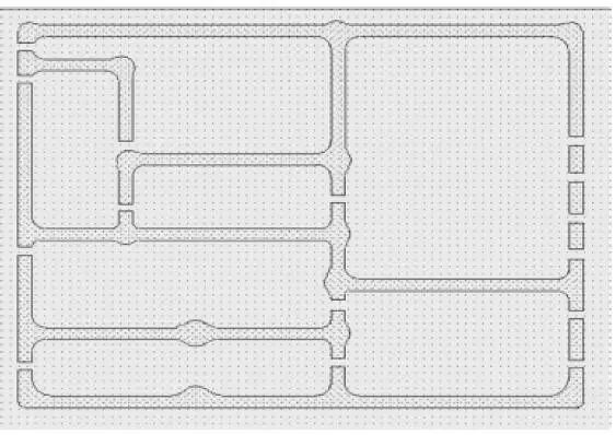
Figure 12 Cavity
The perimeter of the shielding cavity is sealed. Lines leading into the cavity at interfaces generally use stripline or microstrip, while different modules inside the cavity use microstrip. Where different cavities connect, slotting is used, with a slot width of 3 mm, and the microstrip line runs through the middle.
Place 3 mm plated through holes at the corners of the cavity to secure the shielding shell. On each long cavity section, evenly place the same plated through holes to reinforce and support.
The cavity is generally provided with solder mask openings to facilitate soldering of the shielding shell. The cavity is generally more than 2 mm thick. Add two rows of solder-mask-opening via fences on the cavity, with vias staggered, and spacing between vias in the same row of 150 mil.
4 Conclusion
The key to the success of RF circuit PCB design lies in how to reduce circuit radiation and thereby improve anti-interference capability. However, in actual layout and routing, the handling of some issues conflicts with others. Therefore, how to seek a compromise to achieve the optimal overall performance of the entire RF circuit is a problem that designers must consider. All of this requires designers to have certain practical experience and engineering design capabilities. However, no designer can acquire these capabilities overnight. Only by learning from others' experience and continuously exploring and thinking on their own can they make continuous progress. This article summarizes some design experiences from work, which are helpful for improving the anti-interference capability of RF circuit PCBs and helping beginners in RF circuit design avoid unnecessary detours.
About Maxipcb
Maxipcb empowers innovators to turn cutting-edge technologies into reality.We offer one-stop solutions for design, simulation, testing, PCB manufacturing, component procurement and SMT assembly, enabling efficient development, rapid deployment and risk control across the full product lifecycle.
Serving the world in communications, industrial automation, aerospace, automotive, semiconductor and beyond, we build a safer, more connected future together.
