The connection root between a pad and a thin trace is easily weakened by drill misalignment, process variation, and stress. Teardrops add copper precisely at this weak point. However, adding teardrops to the entire board with one click may also suddenly widen the originally uniform geometry of high-speed traces.
The connection root between a pad and a thin trace is easily weakened by drill misalignment, process variation, and stress. Teardrops add copper precisely at this weak point. However, adding teardrops to the entire board with one click may also suddenly widen the originally uniform geometry of high-speed traces. Teardrops are both a mechanical and manufacturing reinforcement and a new electrical structure; the key is not “whether to add them,” but which nodes are worth adding them to and which nodes require caution.
Teardrops Reinforce the Connection Root
When a trace directly intersects a circular pad, the thin trace narrows rapidly near the tangent point. If the drill hole is offset relative to the pad, or etching makes the neck even thinner, the effective copper width may fall below the design value. Teardrops use a gradually widening copper shape to connect the pad and the trace, increasing tolerance to deviation and reducing local stress during repeated thermal cycling or bending. For areas with high current, mechanical stress at the board edge, plug-in connections, or tight annular ring margin, this reinforcement often has clear value.
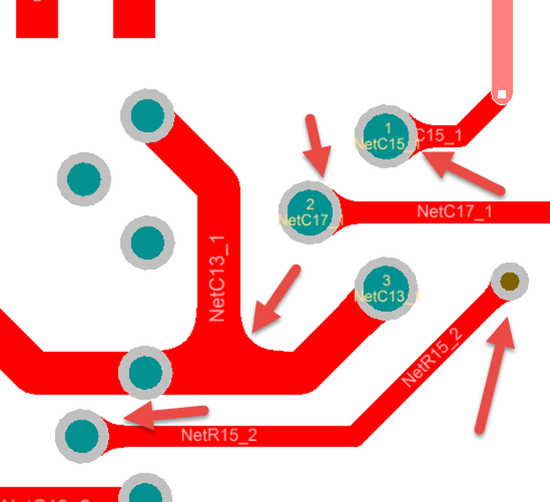
Figure 1: A local routing view shows how teardrops widen the connection neck between the trace and the pad.
Widening the Copper Shape Is Also an Impedance Change
For control lines with slower rising edges, the effect of locally added copper is often not the main issue. For high-speed single-ended or differential lines, a sudden widening of the trace increases local capacitance, and a transition that is too short acts like an impedance step. If the teardrop shapes on both sides of a differential pair or their relationship to the reference plane are inconsistent, asymmetry will also increase. The magnitude of the effect cannot be judged by frequency alone; it also depends on edge rate, geometry, and the total amount of series discontinuity. Dense BGA fan-out is especially prone to accumulation of small effects.
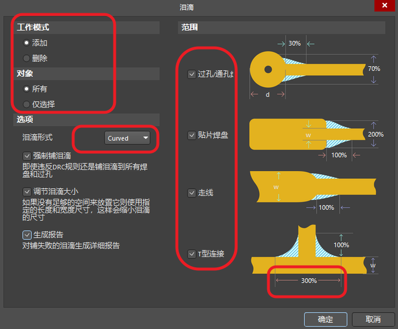
Figure 2: Teardrop parameters determine not only the amount of added copper but also the transition length and local geometry.
Do Not Use One Rule to Cover the Entire Board
A practical approach is to classify first. For power vias, ground vias, high-current pads, board-edge connectors, and mechanically stressed areas, more aggressive teardrops can be set according to the board shop’s drill offset and minimum copper width capabilities. High-speed clocks, serial links, differential pairs, RF feed lines, and sensitive analog nodes should be placed in separate groups. First check whether the pad and trace themselves already meet manufacturing margins. When reinforcement is needed, use longer, symmetrical tapering to reduce abrupt changes, and do not rely on default parameters.
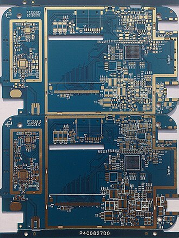
Figure 3: A complete PCB view illustrates that teardrop rules must be reviewed together with stack-up, fan-out, and density.
Answer Questions About High-Speed Nodes with Measurements
To determine whether teardrops affect a link, start with cross-sectional geometry and reflection estimation, then use 3D or 2D electromagnetic tools to compare impedance, return loss, and differential-to-common-mode conversion with and without teardrops. Keep comparable via structures on the prototype board, and observe differences using TDR or eye diagrams under the same excitation. If the result is much smaller than other discontinuities and system margin, the manufacturing benefit can be retained; if the node is already marginal, priority should be given to modifying the pad, trace width, or transition method.
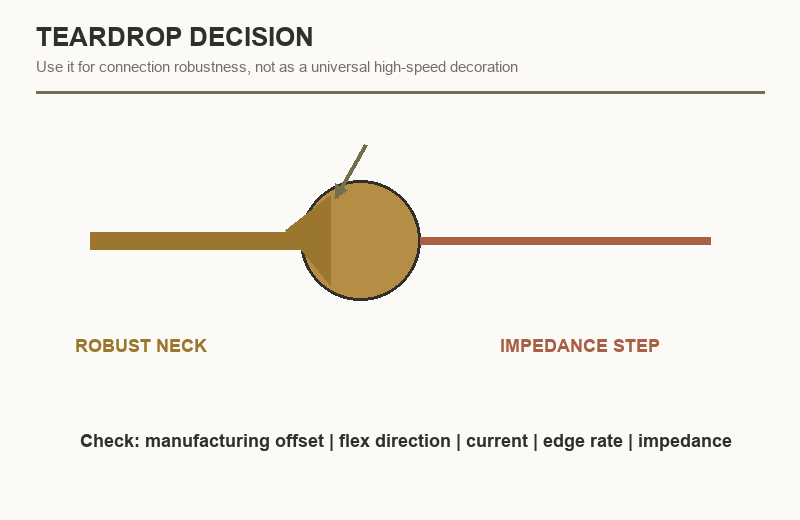
Figure 4: An engineering illustration places mechanical reinforcement and impedance step in the same decision.
Make Teardrops a Traceable Rule
During review, do not only look at a report saying “teardrops added”; record the applicable objects, excluded nets, shape, length, width, and update timing. After modifying vias, changing trace width, or redoing fan-out, old teardrops may remain, overlap, or lose symmetry; they should be regenerated and DRC performed on the effective copper shape. Before outputting manufacturing data, check again the annular ring margin, solder mask opening, copper-to-drill spacing, and symmetry on both sides of the differential pair. In this way, the board shop can understand the design intent, and when changing design tools or design versions, history will not be inherited through a default option.
Also distinguish the connection targets of through vias, blind vias, buried vias, and component pads. Microvias differ from ordinary mechanical holes in copper thickness, pad diameter, and laser drill offset, and in BGA fan-out areas they are also limited by pitch; enlarging teardrops merely to make the pattern look more substantial may squeeze adjacent channels, break differential pair symmetry, or increase the risk of copper-to-copper spacing violations. For ordinary load pads, teardrops cannot replace correct trace width, thermal relief parameters, and current-carrying calculations; for RF and high-speed vias, they cannot be judged only by static impedance values; the effects of return vias, reference plane transitions, and via stubs must also be checked.
When communicating with the board shop, you can request feedback on drill offset, minimum remaining copper width, and annular ring capability, and incorporate the real manufacturing window into the rules. The first-article cross-section can specifically select the smallest annular ring and densest fan-out locations to see whether teardrops truly preserve effective connections. If process stability is sufficient, keeping simple geometry at high-speed nodes is often easier to analyze and reproduce; if process margin is tight, first correct pad dimensions and manufacturing specifications, and then evaluate whether teardrops are necessary. After rule updates, re-output the manufacturing layers and recheck with the production view, because dynamic teardrops displayed by some EDA tools and the final Gerber or ODB++ copper shapes may be affected by version, settings, and object type. The review object should be the final manufacturing data, not a checked option in the interface. In the design library, add notes and net categories to teardrop rules so that later users know why a certain type of net is excluded, rather than seeing a blank and generating teardrops across the entire board again. Only when design intent is preserved in rules and data can it continue to hold when people, versions, and board shops change. If regeneration is required after trace revisions, include this action in the release checklist to avoid old copper shapes remaining in the final manufacturing version.
Teardrops are not a switch for beautifying copper shapes, but a local design feature with mechanical benefits and electrical costs. Classifying by node, setting parameters according to capability, and resolving disputes with measurements are more reliable than adding everywhere or prohibiting everywhere.
Will your teardrop rules exclude high-speed nets, or will you add teardrops across the entire board first and then delete them manually?
About Maxipcb
Maxipcb empowers innovators to turn cutting-edge technologies into reality.We offer one-stop solutions for design, simulation, testing, PCB manufacturing, component procurement and SMT assembly, enabling efficient development, rapid deployment and risk control across the full product lifecycle.
Serving the world in communications, industrial automation, aerospace, automotive, semiconductor and beyond, we build a safer, more connected future together.
