The signal via is only responsible for moving the signal to another layer. Whether the return current can cross layers nearby determines whether this layer transition is complete.
When High-Speed Signals Change Layers, Why Must Return Vias Be Placed Right Next to Them?
The signal via is only responsible for moving the signal to another layer. Whether the return current can cross layers nearby determines whether this layer transition is complete.
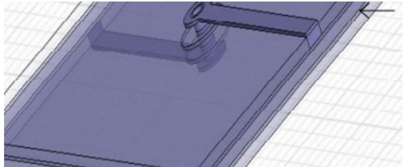
When a high-speed signal changes layers, if one ground via is missing nearby, nothing changes on the schematic, and the board may even boot normally. But at faster edge rates, over longer links, or in EMI testing, impedance dips, insertion loss, and radiation will all emerge together. The problem is not only the signal via; it is that the return current does not change layers synchronously.
Many layout checks focus only on the signal via’s drill diameter, antipad, and stub, while treating the nearby ground via as something to add “if there is room.” At low speed, this may show no difference, but high-speed current does not cross reference planes out of thin air.
The criterion is direct: when signal current changes layers, the return current must also obtain a low-impedance interlayer channel nearby. The farther the ground via is, the longer the return current detour, and the larger the equivalent loop area and parasitic inductance.
First Confirm Which Reference Plane the Signal Actually Changes To
A top-layer microstrip uses the adjacent ground layer as its reference. After transitioning to an inner-layer stripline, the reference plane may become another ground layer, or it may become a power plane. You cannot look only at the layer where the trace is located; you must look at the adjacent planes above and below and the actual return-current conditions in that frequency band.
If both before and after the transition the signal references the same continuous ground plane, the pressure on the return current to cross layers is relatively small. If the reference plane changes, ground vias or inter-plane decoupling are the key to transferring the return current. If there is no nearby high-frequency connection between the power plane and the ground plane, the return current will still take a long detour.
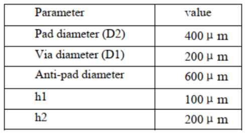
Figure 1 Via drill diameter, pad, and antipad jointly define the local interconnect structure.
The via model in the reference material lists pad, drill diameter, antipad, and layer spacing as parameters of the same structure. It reminds us that a via is not an ideal node, but a three-dimensional interconnect with impedance and electric-field distribution.
Return Vias Must Be Close, but More Is Not Necessarily Better
Ground vias placed nearby can shorten the lateral distance traveled by the return current. For differential-pair layer transitions, return vias can be placed symmetrically on both sides to avoid one line obtaining a shorter return path and breaking local symmetry.
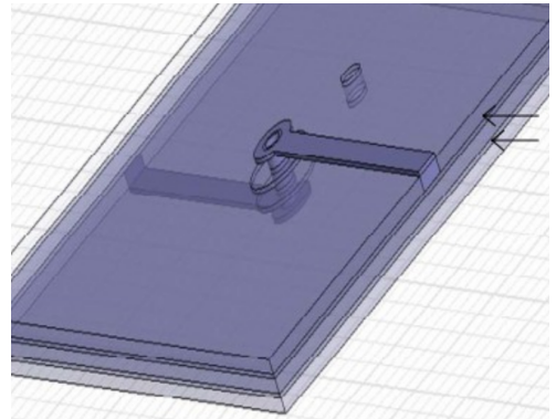
Figure 2 In the 3D model, the relative positions of the signal via and return via change the current path.
“Close” must be considered together with the board shop’s spacing capability and the antipad boundary. If a ground via is too close to the signal via, the antipad and via annular ring may change the local capacitance; if too far, loop inductance increases. Usually, simulation based on the stack-up and target impedance is required, rather than copying a fixed millimeter value.
After the number of ground vias increases to a certain point, the marginal benefit decreases. The curves in the reference material show that both number and spacing change the S-parameters, but the change is not simply linear. First ensure the nearest effective return channel, then consider the number of vias in the fence.
Impedance Anomalies Often Appear at the Instant of Layer Transition
The inductance of the via section, the capacitance of the pad and antipad, plus the return-current detour, together form a local impedance discontinuity. In the time domain, this may be a very short dip or bump; in the frequency domain, it appears as increased reflection and degraded transmission.
Making only the signal via smaller may not solve the problem. If the return current still has to detour to a distant ground via, the main loop inductance has not decreased. Conversely, adjusting ground-via position, plane clearance, and layer-transition structure is often more effective than changing only the signal via.
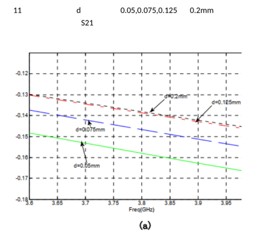
Figure 3 Changes in return-via distance are reflected in the S21 curve.
During simulation or measurement, the signal via, ground vias, and the real reference planes must be modeled together. Extracting only one isolated signal via will miss the most critical return boundary, and the resulting impedance results will be difficult to use for guiding layout.
Layout Review in Four Steps
Step 1: Mark every layer transition along the entire high-speed link. Step 2: Write down the reference plane before and after each transition. Step 3: Measure the position of the nearest ground via or inter-plane decoupling. Step 4: Check whether the return path is cut by slots, splits, or antipads.
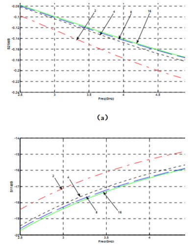
Figure 4 Changes in the number of return vias also change reflection and transmission results.
If the interface board has already been fabricated, TDR can be used to locate impedance changes near the layer transition, and then compare the S-parameters of different return-via schemes. For spectrum problems, observe whether cable common-mode current or near-field strong points decrease with ground-via optimization.
During review, do not ask only “Is there a ground via next to the signal?” Ask whether this ground via is truly connected to the reference planes on both sides, whether the distance is reasonable, and whether the return current still has to cross a large antipad area. This way of asking is closer to the real current.
Also note that inter-plane transfer cannot always be completed by a single ground via. When a signal transitions from a layer referencing a power plane to a layer referencing a ground plane, the actual high-frequency channel may be a nearby decoupling capacitor. If the capacitor is too far from the layer-transition point, the return current will still first detour laterally on the planes.
Via fences cannot replace local return vias either. Ground-via fences at the board edge or near interfaces mainly control fields and boundaries, whereas at a signal layer transition what is needed is a low-impedance connection directly adjacent to that interlayer transition. The two have different functions, and their positions cannot be interchanged.
If the signal crosses a reference-plane split, even if there is a ground via nearby, the return current may not be able to reach the other side. In this case, first adjust the routing or restore a continuous plane; if using a thin copper bridge as a remedy, evaluate its high-frequency impedance. Do not treat DC continuity as high-speed continuity.
Under ideally symmetric conditions, the return currents of differential signals partially cancel each other, but in reality they still couple to the reference plane. Asymmetric layer-transition structures for the two lines, ground vias placed on only one side, or obvious differences in via-to-line distance will all convert differential-mode energy into common-mode energy.
When space is tight in the connector breakout area, first lock down the signal vias and the most critical return vias, then arrange low-speed nets. If ground vias are added only after all routing is completed, usually only options remain that are far from the signal or that break the plane, and later correction costs are higher.
Before mass production, add the net, via type, and solder-mask requirements of return vias to the checklist to prevent them from being mistakenly deleted after panelization, version migration, or library updates. If high-speed issues rely on an engineer’s visual memory, they can easily reappear in the next board revision.
Conclusion
A high-speed signal layer transition is not an action of the signal line alone; it is an interlayer transition completed jointly by the signal and its return current. Treating return vias as optional “supporting actors” means completing only half of the interconnect.
The next time you check a high-speed via, first draw the return-current closed loop along the reference planes, and then decide the distance, number, and antipad of ground vias. If the path cannot be drawn closed, impedance and EMI will sooner or later expose the problem for it.
About Maxipcb
Maxipcb empowers innovators to turn cutting-edge technologies into reality.We offer one-stop solutions for design, simulation, testing, PCB manufacturing, component procurement and SMT assembly, enabling efficient development, rapid deployment and risk control across the full product lifecycle.
Serving the world in communications, industrial automation, aerospace, automotive, semiconductor and beyond, we build a safer, more connected future together.
