Never split the ground plane between analog and digital circuits.
I came across an excellent article on PCB grounding measurement, and the machine translation was unsatisfactory no matter how I read it. So I tried to revise it myself and share it with all of you.
Never split the ground plane between analog and digital circuits.
To explain why this is the case, consider the PCB layout of a mixed-signal board with digital-to-analog (D/A) conversion shown in the figure below, where the ground plane is split between the analog and digital circuit sections. In this case, however, the gap surrounds the analog circuit on three sides.
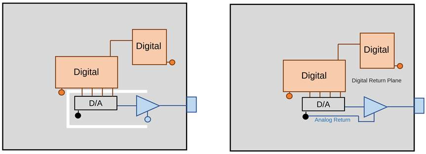
Figure 1. Split Mixed-Signal Board Layout (a) and Optimized Alternative Layout (b)
When considering return currents, although the analog and digital circuit sections are isolated, four digital traces after ground splitting connect the D/A converter to one of the digital components, and these signals also require a return path. These currents must travel from the ground pin of the D/A component to the ground pin of the digital component. The split forces these currents to share the same area of the plane with the analog currents, resulting in mixing of analog and digital signals and defeating the purpose of the split.
Reasons for Prohibiting Ground Split
- For digital and analog signals operating at frequencies above approximately 100 kHz, the return current on the ground plane is confined to the area directly beneath the signal trace.
- Even at frequencies of kHz or lower, the resistance of the circuit board ground plane is less than 1 mΩ per square. For example, 10A of current flowing through a 1 mΩ resistor will generate a voltage of 10mV, which is negligible in some scenarios.
- In cases where mV-level coupling cannot be tolerated, it is better to distribute the return paths on different layers.
Single-Point and Multi-Point Grounding
As shown in Figure 2, there are two possible paths for the analog return current. It can return on the trace or on the plane. The current will be distributed according to the resistance of each path, allowing a large amount of analog current to return to the plane. Similarly, some digital current will flow on the return path of the analog current.
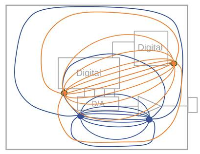
Figure 2 Approximate Return Current Distribution on the Ground Plane
In general, if two current return paths are connected at more than one point, they will not be isolated at low frequencies. Single-point grounding is a critical concept in Electromagnetic Compatibility (EMC), although it is often misunderstood by designers who fail to correctly distinguish between the concepts of current return path and grounding.
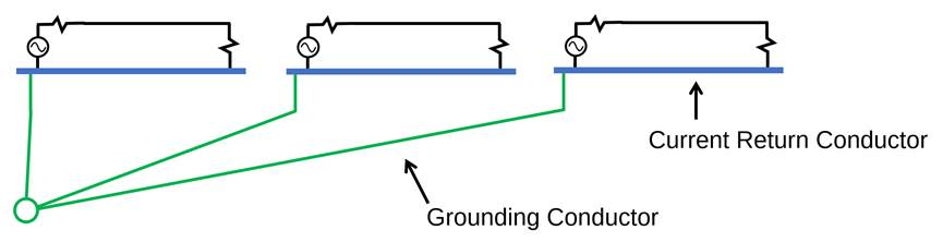
Figure 3. Single-Point Grounding
Figure 3 illustrates the concept of single-point grounding, where isolated circuits or systems are connected to a single point through a non-current-carrying grounding conductor.
Figure 4 shows another implementation, where the grounding conductors are connected at multiple points but still referenced to a single point. One example is the power supply grounding in a building, where each grounded device has a dedicated wired path to the building's electrical service, and connecting the grounding conductors at multiple points does not reduce the effectiveness of the grounding scheme.
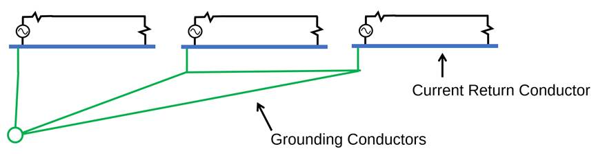
Figure 4. Alternative Implementation of Single-Point Grounding
While single-point grounding is an important concept for ensuring that isolated circuits have the same zero-volt reference, it does not work if the grounding conductors carry signal or power currents.
In Figure 5, the middle and right circuits are not isolated. The current returning from the load to the source of the middle circuit can now choose to return via the intended blue conductor, or back to the middle circuit through the "single-point" ground via the additional connection to the right circuit.
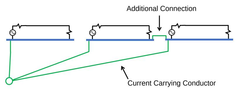
Figure 5. This Is Not Single-Point Grounding
It is important to remember that single-point grounding is a critical strategy for ensuring that isolated circuits and devices have the same zero-volt reference. On the other hand, single-point current return is often the root cause of severe electromagnetic coupling problems.
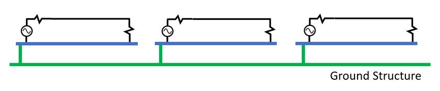
Figure 6. Multi-Point Grounding
An alternative to the single-point grounding strategy is the multi-point grounding strategy, as shown in Figure 6.
Systems using a ground structure typically connect circuits and modules that are not isolated from the ground structure at multiple points. A simple example is demonstrated in Figure 7. In this case, the connection between the middle and right circuits allows low-frequency return currents to flow on the ground structure. At these frequencies, the structure would be more accurately described as a current return structure. When developing a grounding strategy, it is important to recognize that a conductive structure can provide a grounding function at some frequencies and a current return function at others.

Figure 7. Hybrid Grounding Strategy
Grounding Strategy
- An appropriate current return strategy usually focuses on providing a low-inductance path for high-frequency currents and maintaining control over the low-frequency current path.
- A correct grounding strategy focuses on identifying and protecting the zero-volt reference voltage source for each circuit and system.
- Define the ground structure. At the system level, the ground structure is always the metal enclosure or frame; at the board level, if the board is connected to the frame, the board ground should be the point where the connection occurs.
- All large metal objects shall be connected to the ground structure. If this is not possible, they must be sufficiently isolated from the ground structure to ensure that severe coupling does not occur.
About Maxipcb
Maxipcb empowers innovators to turn cutting-edge technologies into reality.
We offer one-stop solutions for design, simulation, testing, PCB manufacturing, component procurement and SMT assembly, enabling efficient development, rapid deployment and risk control across the full product lifecycle.Serving the world in communications, industrial automation, aerospace, automotive, semiconductor and beyond, we build a safer, more connected future together.
