Question: Why is PCB Panelization Required?
Panelization is mainly implemented to meet production requirements. Some PCBs are too small to meet fixture manufacturing specifications, so they must be combined into panels for production.
Panelization also improves the efficiency of SMT mounting and soldering; for example, multiple PCBs can be soldered in a single SMT pass.
Meanwhile, it reduces costs. For some special-shaped PCBs, panelization minimizes material waste and enhances board area utilization.
Defect Case of Zero-spacing Panelization
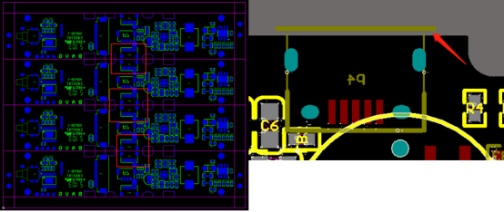
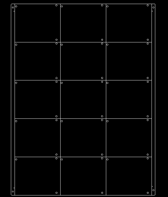
Component package silkscreens on the PCB exceeded the board edge during design, and this issue was not checked during panelization. As a result, zero-spacing panelization caused component interference, which impaired SMT mounting.
Impact of the Problem
Components exceeding the board edge cannot be assembled after zero-spacing panelization, delaying the product development cycle.
Forced assembly (e.g., assembling half of the adjacent components on the same side while leaving the other half unassembled) will result in 50% product scrap.
After zero-spacing panelization of components exceeding the board edge, even if through-hole assembly is barely feasible, component damage will occur during depanelization, leading to greater cost losses.
Applicable Methods of PCB Panelization
-
CNC Routing + V-Cut Panelization
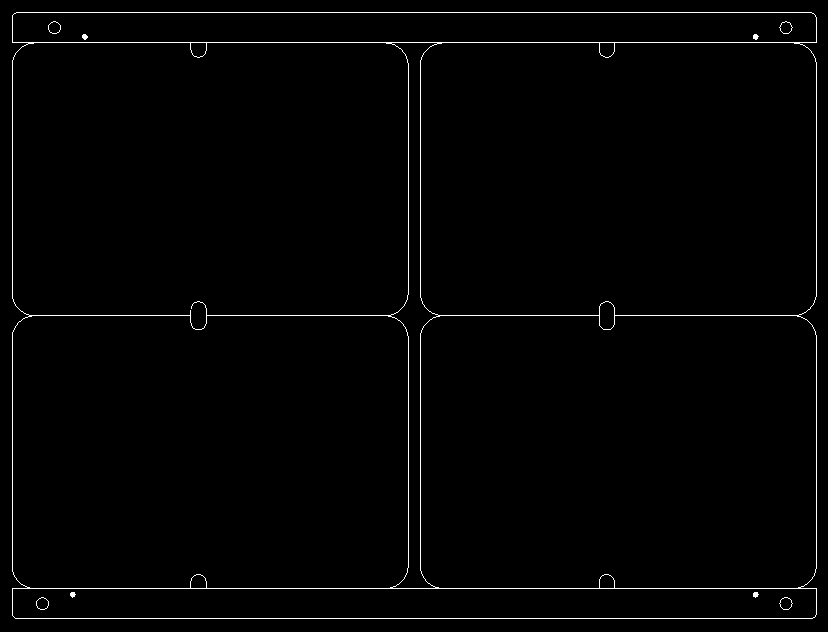
This method combines CNC routing and V-groove processing. It is suitable for PCBs with components along the board edges that do not allow zero-spacing panelization. Panelization is performed with process edges added; V-Cut processing is applied to the process edges at both ends, and the middle spacing is routed out to facilitate component soldering. Otherwise, components on adjacent board edges will interfere with each other and fail assembly and soldering.
-
Stamp Hole Bridging Panelization
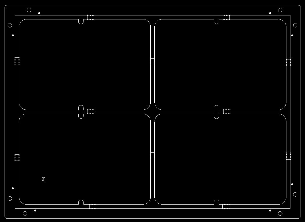
Stamp holes are a bridging method for panelization. Stamp hole bridging resolves issues that cannot be addressed by V-Cut bridging. For example, circular PCBs and irregular-shaped PCBs that cannot be processed with V-Cut must adopt stamp hole bridging for panelization.
-
V-Cut Bridging Panelization
V-Cut bridging panelization is suitable for regular-shaped PCBs. Since the V-Cut blade cannot turn, V-Cut positions must be straight lines. It should also be noted that panelization with V-Cut is not allowed where components are close to the board edge; otherwise, assembly and soldering will be affected.
-
Panelization Without Process Edges
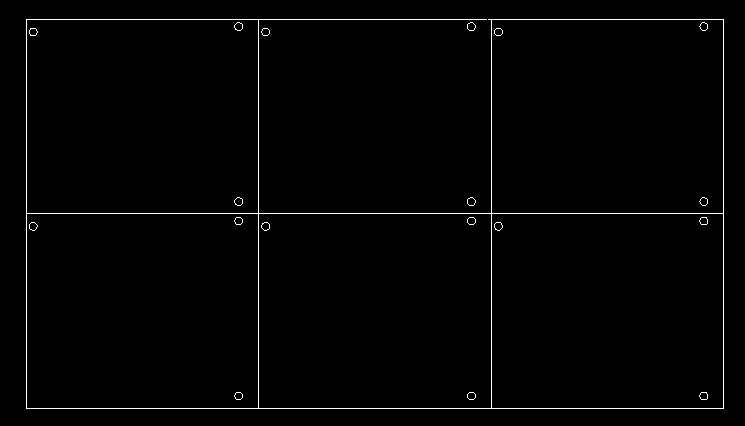
To maximize material utilization, small PCBs are often panelized without process edges. However, no components shall be placed at the board edge along the V-Cut line. If components are close to the board edge, process edges with reserved spacing are recommended for panelization; otherwise, component assembly and solderability will be impaired.
 About Maxipcb
Maxipcb empowers innovators to turn cutting-edge technologies into reality.
We offer one-stop solutions for design, simulation, testing, PCB manufacturing, component procurement and SMT assembly, enabling efficient development, rapid deployment and risk control across the full product lifecycle.Serving the world in communications, industrial automation, aerospace, automotive, semiconductor and beyond, we build a safer, more connected future together.