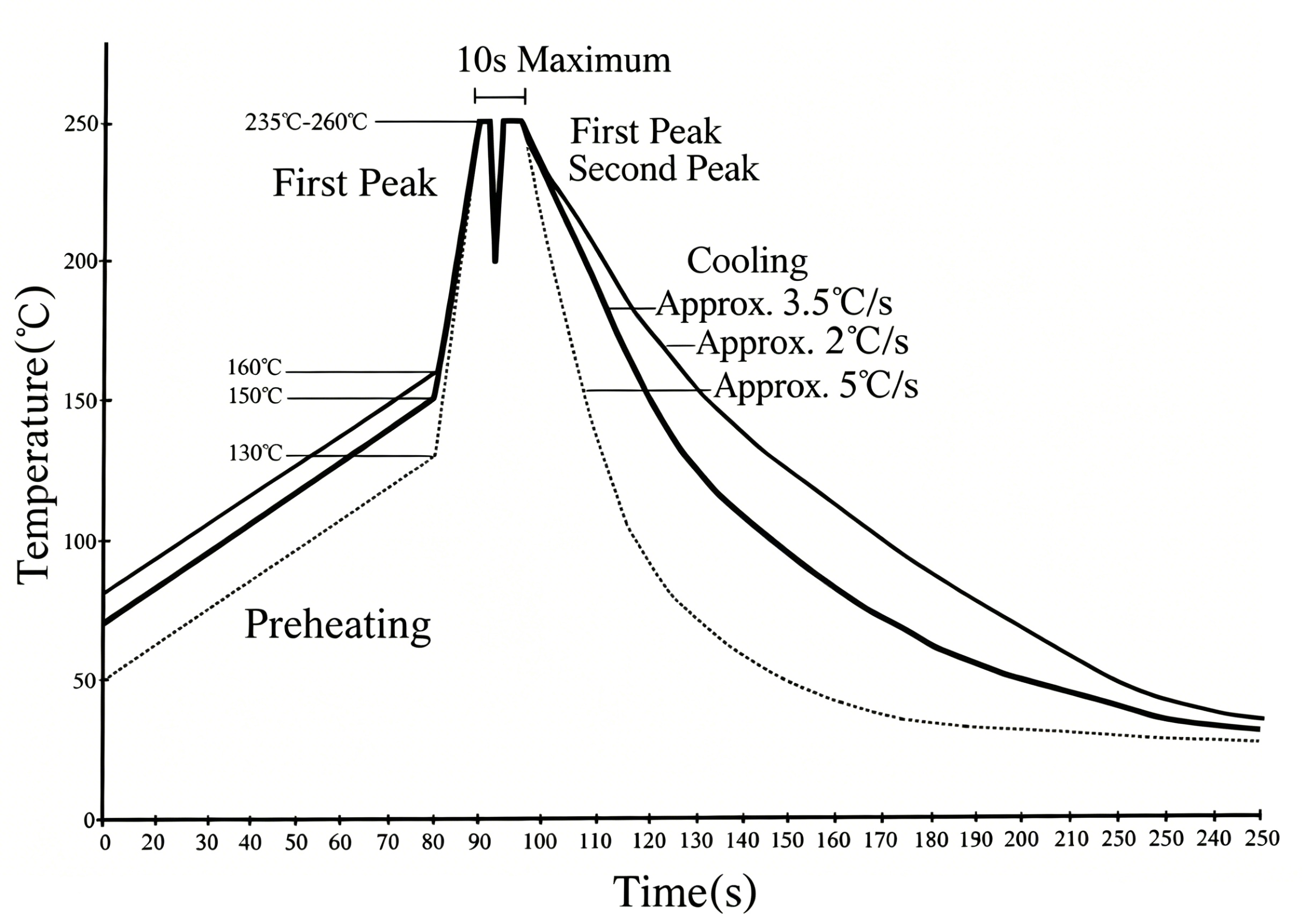
When a PCB enters the preheating zone (drying zone), solvents and gases in the solder paste evaporate. Meanwhile, the flux in the solder paste wets the pads and connector pins; the solder paste softens, collapses, and covers the pads, isolating the connector pins from oxygen.
When a PCB enters the preheating zone (drying zone), solvents and gases in the solder paste evaporate. Meanwhile, the flux in the solder paste wets the pads and connector pins; the solder paste softens, collapses, and covers the pads, isolating the connector pins from oxygen.
→ When the PCB enters the soaking zone, the PCB and connector pins are fully preheated to prevent damage caused by the PCB suddenly entering the soldering zone.
→ When the PCB enters the reflow zone, the temperature rises rapidly to melt the solder paste. Liquid solder wets, diffuses, flows, or reflows and mixes with the PCB pads and connector pins to form solder joints.
→ The PCB enters the cooling zone to solidify the solder joints. Reflow soldering is completed at this stage.
Conventional Soldering Temperature of Reflow Soldering
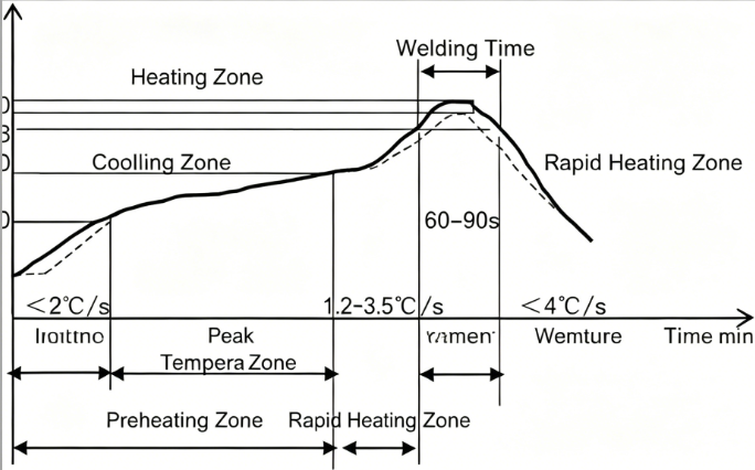
Temperature ramp-up rate: 1.2~3.5°C/s
Peak temperature
Duration: 60~90s
Temperature profile zones: Preheating zone, soaking zone, soldering zone (ramp-up rate 2~35°C/s), cooling zone (ramp-down rate <4°C/s)
Duration: 60~90s
Sub-zones: Preheating zone, rapid temperature rise zone
Preheating zone: Room temperature to 150℃
Soaking zone: 150℃~200℃
Reflow zone: 220℃, maximum temperature 249℃
Cooling zone: Cooled from 220℃ to approximately 150℃
Note: The soldering profile varies for different products; consult the relevant manufacturer for details.
Soldering Principle of Wave Soldering
Wave soldering is a soft soldering process that uses an electric or electromagnetic pump to spray molten soft solder (lead-tin alloy) into a designed solder wave; nitrogen can also be injected into the solder bath to form the wave. A printed circuit board pre-assembled with connectors passes through the solder wave to achieve mechanical and electrical connection between connector pins and PCB pads.
Conventional Soldering Temperature of Wave Soldering
- Preheating zone: Bottom temperature of the PCB ranges from 90-120℃
- Soldering: Solder joint temperature ranges from 245±10℃
- PCB temperature at the oven outlet: Controlled below 100℃
Note: The soldering profile varies for different products; consult the relevant manufacturer for details.
Causes of Warpage
After injection molding, during the cooling process of a connector, the outer portion shrinks while the interior remains at a high temperature and shrinks more slowly. Upon cooling, tensile and compressive stresses form between the exterior and interior of the connector. Part of these stresses causes warpage, and the remainder remains inside the connector as residual stress. When the connector undergoes reflow soldering, the residual stress is released, ultimately resulting in thermal warpage and deformation of the connector.
About Maxipcb
Maxipcb empowers innovators to turn cutting-edge technologies into reality.
We offer one-stop solutions for design, simulation, testing, PCB manufacturing, component procurement and SMT assembly, enabling efficient development, rapid deployment and risk control across the full product lifecycle.Serving the world in communications, industrial automation, aerospace, automotive, semiconductor and beyond, we build a safer, more connected future together.