In the previous article, we introduced the basic approach to the mounting PCB layout of a boost DC/DC converter, namely the current paths related to switching. Before explaining the PCB board layout of a boost DC/DC converter separately, this article first introduces the overall steps and key points of the PCB board layout of a boost DC/DC converter.
In the previous article, we introduced the basic approach to the mounting PCB layout of a boost DC/DC converter, namely the current paths related to switching. Before explaining the PCB board layout of a boost DC/DC converter separately, this article first introduces the overall steps and key points of the PCB board layout of a boost DC/DC converter.
Steps for the Mounting PCB Layout of a Boost DC/DC Converter
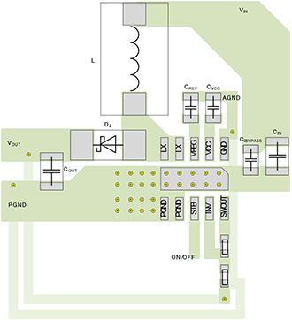
The steps for the mounting PCB layout are roughly as follows. The figure on the right is a schematic illustration.
Place the input capacitors CIN and CIBYPASS near the IC.
Make the ground loop between the output capacitor COUT and the switching MOSFET as small as possible.
Place the output capacitor COUT, freewheeling diode D2, and inductor L as close as possible, and place them on the same side.
In particular, keep the copper foil pattern area of inductor L from being too large, so that radiated noise from the switching node is reduced.
Provide thermal vias when necessary.
Keep the feedback path as far as possible from the vicinity of the output capacitor COUT, and route it as far as possible from noise sources such as the output capacitor COUT and freewheeling diode D2.
Some devices require external compensation components RC and CC. Place these components near the IC ground.
When a feedback divider is required, place it near the IC ground.
About Maxipcb
Maxipcb empowers innovators to turn cutting-edge technologies into reality.We offer one-stop solutions for design, simulation, testing, PCB manufacturing, component procurement and SMT assembly, enabling efficient development, rapid deployment and risk control across the full product lifecycle.
Serving the world in communications, industrial automation, aerospace, automotive, semiconductor and beyond, we build a safer, more connected future together.
