Current Paths of Boost DC/DC Converters
Not only for boost DC/DC converters, but in PCB layout design for many products, it is very important to understand the current paths and characteristics of the circuit. Before going into the specific layout explanation, let’s first look at the current paths of a boost DC/DC converter.
Current Paths of Boost DC/DC Converters
Not only for boost DC/DC converters, but in PCB layout design for many products, it is very important to understand the current paths and characteristics of the circuit. Before going into the specific layout explanation, let’s first look at the current paths of a boost DC/DC converter.
Current path when switching transistor Q2 is ON
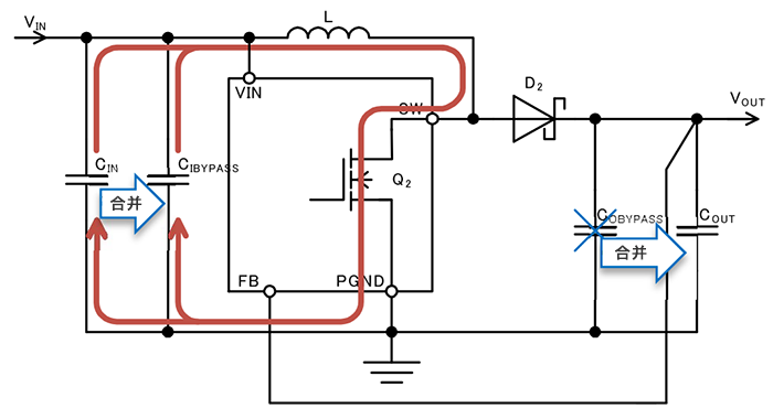
The figure below is a schematic diagram of a boost DC/DC converter. The red lines indicate the main currents flowing when switching transistor Q2 is ON. CIBYPASS is a high-frequency decoupling capacitor, usually a small-capacity ceramic capacitor. CIN is mainly a stabilizing capacitor and has a larger capacitance. At the instant switching transistor Q2 turns on, most of the rapidly flowing current comes from CIBYPASS, followed by CIN. When the input current is not very large, CIN can be combined with CIBYPASS and reused as one capacitor. The slowly changing current comes from the input power supply. During this period, energy is stored in inductor L.
Current path when switching transistor Q2 is OFF
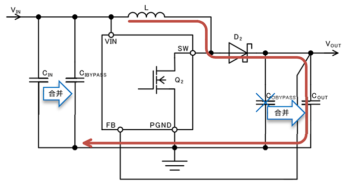
Next, look at the current state when switching transistor Q2 is OFF (red lines in the figure). The role of inductor L is to maintain the previous current value even when switching transistor Q2 is OFF. The left end of inductor L is fixed at VIN and continuously supplies current to VOUT to increase the voltage, so VOUT is higher than VIN (boost operation). Therefore, the longer switching transistor Q2 is ON, the more energy is stored in inductor L, and the more power can be output. However, if the ON time of switching transistor Q2 is unnecessarily extended, the time for supplying power to the output decreases, and efficiency worsens. Therefore, the maximum ON/OFF time ratio (duty cycle) is limited. In circuits with small output current, if COUT uses a ceramic capacitor with good frequency characteristics, the high-frequency decoupling capacitor CBYPASS can be reused.
Current difference between switching transistor Q2 ON and OFF
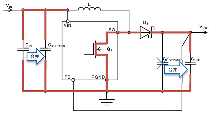
Finally, look at the current difference between switching transistor Q2 ON and OFF (red lines in the figure). Whenever switching transistor Q2 changes from OFF to ON and from ON to OFF, the current in the path indicated by the red lines changes sharply. Because this system changes very abruptly, waveforms containing many harmonics appear. The layout of this differential system is the key to PCB layout and requires extra attention.
About Maxipcb
Maxipcb empowers innovators to turn cutting-edge technologies into reality.We offer one-stop solutions for design, simulation, testing, PCB manufacturing, component procurement and SMT assembly, enabling efficient development, rapid deployment and risk control across the full product lifecycle.
Serving the world in communications, industrial automation, aerospace, automotive, semiconductor and beyond, we build a safer, more connected future together.
