
The issue of EMC design in PCBs is probably a major headache for many electronic hardware engineers. For example: How should EMC be considered in PCB stackup? When designing for EMC with boards of different layer counts, do the considerations differ?
PCB Layer Stackup EMC Series Knowledge
Should‑have PCB Stackup EMC Series Knowledge (Part 2)
If you don't consider EMC during PCB stackup, you'll be left with "too hard" after finishing.
Considering everyone's needs, Sister Lu has compiled some strategies for [EMC design in PCBs], hoping they will be helpful to you...
I. Component Placement
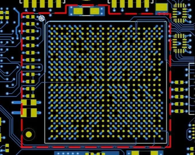
In the PCB design process, from an EMC perspective, three main factors should be considered first: the number of I/O pins, component density, and power dissipation. A practical rule is that chip components should occupy 20% of the substrate area, and the power dissipation per square inch should not exceed 2 W.
In terms of component arrangement, the principle is to place related components as close as possible, separate digital circuits, analog circuits, and power supply circuits, and separate high‑frequency circuits from low‑frequency circuits.
Noise‑prone components, low‑current circuits, high‑current circuits, etc., should be kept as far away from logic circuits as possible. Clock circuits and high‑frequency circuits, which are major sources of interference and radiation, should be arranged separately and kept away from sensitive circuits. I/O chips should be located near the I/O exit points of the hybrid circuit package.
High‑frequency components should have their interconnections as short as possible to reduce distributed parameters and mutual electromagnetic interference. Susceptible components should not be too close to each other, and inputs and outputs should be kept far apart. Oscillators should be placed as close as possible to the clock‑using chips and away from signal interfaces and low‑level signal chips.
Components should be parallel or perpendicular to one edge of the substrate, and preferably arranged in parallel rows. This not only reduces distributed parameters between components but also conforms to hybrid circuit manufacturing processes, making production easier.
On the hybrid circuit substrate, the power and ground lead‑out pads should be arranged symmetrically, and it is best to distribute many power and ground I/O connections evenly. The die‑attach area for bare chips should be connected to the most negative potential plane.
When using multilayer hybrid circuits, the layer arrangement varies with the specific circuit, but generally has the following characteristics:
(1) Power and ground layers are assigned to inner layers, acting as shielding layers that effectively suppress common‑mode RF interference inherent to the board and reduce the distributed impedance of the high‑frequency power supply.
(2) The power plane and ground plane on the board should be as close as possible to each other, with the ground plane generally above the power plane. This allows the inter‑layer capacitance to serve as a smoothing capacitor for the power supply, while the ground plane shields the radiated current distributed on the power plane.
(3) Routing layers should be placed adjacent to power or ground planes to achieve flux cancellation.
II. PCB Routing
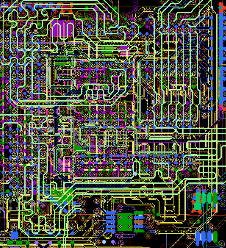
In circuit design, designers often focus only on increasing routing density or achieving uniform layout, neglecting the impact of routing on interference prevention. This causes a large number of signals to radiate into space, creating interference and potentially leading to more electromagnetic compatibility problems.
Therefore, good routing is key to a successful design.
1. Ground routing
The ground line is not only the reference point for circuit operation but also serves as a low‑impedance return path for signals.
The most common interference on ground lines is ground‑loop interference caused by ground‑loop currents. Solving this type of problem solves most electromagnetic compatibility issues.
Noise on the ground line mainly affects the ground level of digital circuits, and when digital circuits output a low level, they are particularly sensitive to ground noise.
Interference on the ground line can not only cause circuit malfunctions but also generate conducted and radiated emissions. Therefore, the key to reducing these interferences is to minimise the ground impedance (for digital circuits, reducing ground inductance is especially important).
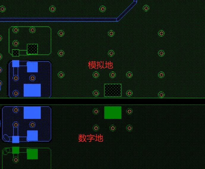
Key points for ground routing:
(1) Separate ground lines should be provided for digital and analog circuits according to different supply voltages.
(2) The common ground line should be made as wide as possible. In multilayer thick‑film processes, a dedicated ground plane can be used, which helps reduce loop area and lowers the antenna efficiency of the return path, while also serving as a shield for signal lines.
(3) Comb‑shaped ground lines should be avoided, as this structure creates large signal return loops, increases radiation and susceptibility, and the common impedance between chips may cause circuit malfunctions.
(4) When multiple chips are mounted on the board, significant potential differences may appear on the ground line. The ground line should be designed as a closed loop to improve the circuit's noise margin.
(5) For boards with both analog and digital functions, analog ground and digital ground are usually separated and connected only at the power supply.
2. Power supply routing
Generally, apart from interference directly caused by electromagnetic radiation, interference via the power lines is the most common. Therefore, power line routing is also important, and the following rules should generally be followed:
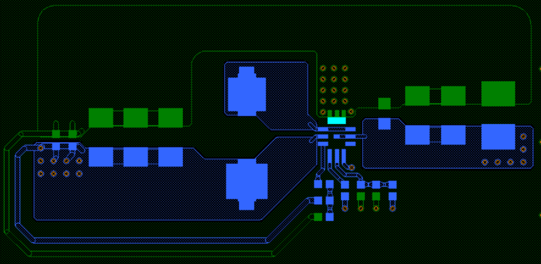
(1) Power lines should be routed as close as possible to ground lines to reduce the power supply loop area, minimise differential‑mode radiation, and help reduce circuit crosstalk. Supply loops for different power rails should not overlap.
(2) In multilayer processes, analog and digital power supplies should be separated to avoid mutual interference. Do not place digital power planes overlapping analog power planes, as this creates coupling capacitance and degrades isolation.
(3) The power plane and ground plane can be isolated with a full dielectric layer. When frequencies and speeds are very high, a dielectric material with low dielectric constant should be used. The power plane should be close to the ground plane and placed below it, so that the ground plane shields the radiated current distributed on the power plane.
(4) Decoupling should be provided between the chip's power pin and ground pin. Decoupling capacitors of 0.01 µF chip capacitors should be placed as close to the chip as possible to minimise the decoupling loop area.
(5) When using surface‑mount chips, choose those with power and ground pins as close together as possible. This further reduces the power supply loop area for the decoupling capacitor and helps achieve electromagnetic compatibility.
3. Signal line handling
When using a single‑layer thin‑film process, a simple and practical method is to first route the ground lines, then route critical signals (such as high‑speed clock signals or sensitive circuits) close to their ground return paths, and finally route the remaining circuits.
Signal lines are best arranged according to the signal flow direction, so that the signals on the board flow smoothly.
To minimise EMI, keep signal lines as close as possible to their return signal lines, so that the loop area is as small as possible to avoid radiation interference.
Low‑level signal channels should not be placed near high‑level signal channels or unfiltered power lines. Noise‑sensitive traces should not run parallel to high‑current, high‑speed switching lines. If possible, route all critical traces as striplines. Incompatible signal lines (digital vs. analog, high‑speed vs. low‑speed, high‑current vs. low‑current, high‑voltage vs. low‑voltage, etc.) should be kept far apart and not routed in parallel.
Crosstalk between signals is extremely sensitive to the length of adjacent parallel traces and the spacing between them. Therefore, increase the spacing between high‑speed signal lines and other parallel signal lines as much as possible and reduce the parallel length.
The inductance of a trace is proportional to its length and the logarithm of its length, and inversely proportional to the logarithm of its width.
Therefore, traces should be as short as possible. Address lines or data lines for the same component should be kept as close in length as possible. I/O‑type traces should avoid adjacent parallel runs; it is best to insert ground lines between them to effectively suppress crosstalk. Low‑speed signals can tolerate relatively higher routing density, while high‑speed signals should use as low a density as possible.
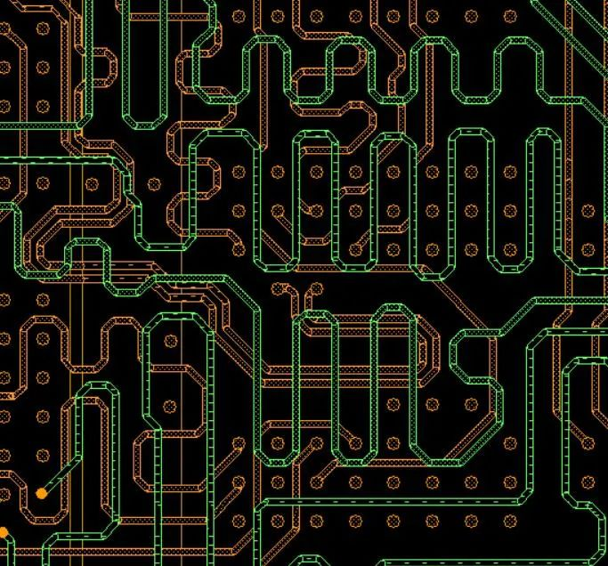
In multilayer thick‑film processes, in addition to following the single‑layer routing rules, the following should also be noted:
-
Design a dedicated ground plane whenever possible, and place signal layers adjacent to ground layers. When this is not feasible, place a ground line near high‑frequency or sensitive circuits.
-
Signal traces on different layers should run perpendicular to each other to reduce electric‑ and magnetic‑field coupling between lines. On the same layer, keep a certain spacing between signal lines and, ideally, isolate them with corresponding ground return lines to reduce crosstalk.
-
Each high‑speed signal line should be confined to a single layer. Signal lines should not be too close to the substrate edge, as this causes characteristic impedance changes and also tends to generate fringing fields that increase outward radiation.
4. Clock circuit handling
Clock circuits occupy an important position in digital circuits and are also a major source of electromagnetic radiation.
A clock signal with a 2 ns rise time can radiate energy with a spectrum reaching 160 MHz. Therefore, designing the clock circuit well is key to ensuring the overall electromagnetic compatibility of the circuit.
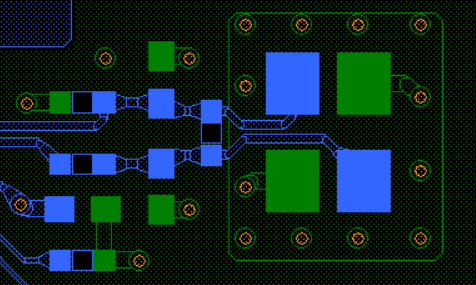
Key points for clock circuit layout:
(1) Do not use a daisy‑chain structure to distribute clock signals; instead, use a star structure, where all clock loads are directly connected to the clock power driver.
(2) Keep the traces connecting the crystal oscillator input/output pins as short as possible to reduce noise interference and the effect of parasitic capacitance on the crystal.
(3) The ground line for the crystal capacitor should be connected to the device with the widest and shortest possible trace. Use as few vias as possible for the digital ground pin closest to the crystal.
III. Process and Component Selection
Hybrid integrated circuits can be fabricated using three manufacturing processes: single‑layer thin‑film, multilayer thick‑film, and multilayer co‑fired thick‑film.
The thin‑film process can produce small‑size, low‑power, and high‑current‑density components required for high‑density hybrid circuits. It offers high quality, stability, reliability, and flexibility, making it suitable for high‑speed, high‑frequency, and high‑packaging‑density circuits, but it can only provide single‑layer routing and is relatively costly.
The multilayer thick‑film process can produce multilayer interconnect circuits at a lower cost. From an EMC perspective, multilayer routing reduces board radiation and improves the board's immunity to interference.
Because dedicated power and ground layers can be provided, the distance between signal and ground is only the inter‑layer spacing. This minimises the return loop area for all signals on the board, effectively reducing differential‑mode radiation.
Among these, the multilayer co‑fired thick‑film process offers more advantages and is currently the mainstream technology for passive integration. It allows more layers of routing, easier embedding of passive components, higher assembly density, and good high‑frequency and high‑speed transmission characteristics.
In addition, it is compatible with thin‑film technology, and the combination of the two can achieve higher assembly density and better performance in hybrid multilayer circuits.
Active devices in hybrid circuits are generally bare chips. When bare chips are not available, corresponding packaged chips can be used. To obtain the best EMC characteristics, surface‑mount chips are preferred.
When selecting chips, choose the slowest clock that meets the product specifications. If HC can be used, do not use AC; if CMOS4000 is sufficient, do not use HC. Capacitors should have low equivalent series resistance (ESR) to avoid significant signal attenuation.
Hybrid circuit packages can use Kovar bases and lids with parallel seam welding, which provide good shielding.