Printed Circuit Board (PCB) routing plays a vital role in high-speed circuit design, yet it is often completed in the later stages of the overall design process. A vast number of technical documents have been published covering various challenges of high-speed PCB routing. This article discusses high-speed circuit routing from a practical perspective.
Printed Circuit Board (PCB) routing plays a vital role in high-speed circuit design, yet it is often completed in the later stages of the overall design process. A vast number of technical documents have been published covering various challenges of high-speed PCB routing. This article discusses high-speed circuit routing from a practical perspective. It aims to help novice designers recognize key considerations during high-speed PCB layout, and also serves as a review material for engineers who have not engaged in PCB routing for a long time. Limited by layout space, this paper cannot elaborate on every detail, but it focuses on core techniques that effectively improve circuit performance, shorten design cycles and reduce revision workload.
Although the content is mainly oriented to circuits using high-speed operational amplifiers, the discussed principles and methods are universally applicable to most other high-speed analog circuits. When operational amplifiers operate at radio frequency (RF) bands, circuit performance is heavily dependent on PCB routing. A well-designed high-performance circuit on schematic may end up with mediocre performance due to careless routing. Full consideration of critical details throughout the routing process helps deliver circuit performance as expected.
Schematic Design
A well-designed schematic does not guarantee perfect routing, whereas excellent routing always starts with a high-quality schematic. Schematic design requires careful deliberation and full consideration of the overall signal flow of the circuit. If signals flow logically and stably from left to right on the schematic, the PCB layout shall follow the same signal routing logic.
Include as much useful information as possible on the schematic. When circuit designers are unavailable, technicians and engineers responsible for troubleshooting will greatly benefit from comprehensive schematic notes.
Apart from standard reference designators, power consumption ratings and tolerance values, additional information can be added to upgrade a regular schematic to a professional one, including: waveform diagrams, mechanical dimensions of enclosures, trace length requirements, reserved blank areas, component placement side markers, adjustment parameters, component value ranges, heat dissipation notes, controlled-impedance trace specifications, annotations, brief circuit operation descriptions and other supplementary details.
Do Not Fully Rely on Others’ Layout Work
If you assign routing work to other engineers, set aside sufficient time to thoroughly review their designs. Minor precautions at an early stage can avoid massive rework later on. Do not assume that routing engineers can fully understand your design intent. Your guidance and feedback are critical in the early phase of routing. The more detailed information you provide and the more you participate during the routing process, the better the final PCB will be.
Set interim checkpoints for routing progress and conduct regular reviews based on the expected layout. This closed-loop management prevents the layout from deviating from requirements and minimizes rework risks.
Detailed instructions for routing engineers shall cover: a brief description of circuit functions, PCB sketches marking input and output positions, PCB stackup information (including board thickness, layer count, and details of each signal layer and ground plane such as power distribution, ground routing, analog signals, digital signals and RF signals), signal allocation for each layer, placement requirements for key components, exact positions of bypass components, critical trace definitions, traces requiring impedance control, traces needing length matching, component dimensions, spacing requirements between specific traces and components, and component placement sides (top or bottom of the PCB). Never worry about providing excessive information — insufficient information will cause problems, while detailed guidance will not.
Practical Experience Sharing
About a decade ago, I designed a multilayer surface-mount PCB with components mounted on both sides. The board was fixed to a gold-plated aluminum enclosure with multiple screws due to strict shock resistance specifications. Pins for bias feedthrough passed through the PCB and were soldered to internal traces, forming a complex assembly. Some components on the board were used for Setup and Test (SAT). I clearly specified their placement locations, but all these SAT components were mounted on the bottom side of the PCB. Later, product engineers and technicians had to disassemble the entire assembly repeatedly to complete tests, which caused great inconvenience. I have avoided similar mistakes ever since.
Component Placement
In PCB design, placement determines overall performance. The layout of the entire circuit, the position of individual components and adjacent circuit modules are all extremely important.
In most cases, the positions of inputs, outputs and power interfaces are predefined, leaving flexible layout space for intermediate circuits. This is why proper handling of routing details can bring significant performance improvements. Start layout planning with key components and take both the circuit function and overall PCB layout into account. Defining the placement of critical components and signal paths at the initial stage helps achieve design targets, cut costs, reduce work pressure and shorten the development cycle by getting the design right at the first attempt.
Power Supply Bypassing
Power supply bypassing for noise reduction is a key part of PCB design for both high-speed operational amplifiers and other high-speed circuits. Two mainstream configurations are widely used for op-amp power bypassing.
Power Pin to Ground
This is the most effective solution for most applications. Connect multiple capacitors in parallel directly from the op-amp power pins to the ground plane. Generally, two parallel capacitors are sufficient, while extra capacitors can bring performance gains for certain circuits.
Parallel capacitors with different capacitance values ensure that the AC impedance of power pins remains low across a wide frequency range, which is especially critical at the roll-off frequency of the op-amp Power Supply Rejection (PSR). Bypass capacitors compensate for degraded PSR performance. A low-impedance ground path maintained over multiple frequency decades prevents unwanted noise from entering the op-amp.
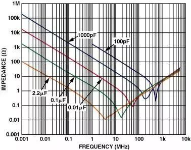 Figure 1 Impedance characteristics of capacitors versus frequency
Follow the rules below for capacitor placement: Start with the smallest capacitor. Mount the capacitor with the minimum capacitance and smallest package on the same PCB side as the op-amp, and place it as close to the chip as possible. Connect the capacitor’s ground terminal to the ground plane via the shortest leads or traces. Arrange this ground connection near the op-amp load terminal to mitigate interference between power and ground paths.
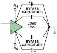 Figure 2 Parallel bypass capacitors for power and ground connections
Apply the same placement rules for capacitors with larger capacitance values. A typical combination is a 0.01 µF ceramic capacitor paired with a 2.2 µF (or higher) electrolytic capacitor with low Equivalent Series Resistance (ESR). The 0.01 µF capacitor in 0508 package features low series inductance and excellent high-frequency performance.
Positive Power Pin to Negative Power Pin
The second configuration connects one or more bypass capacitors between the positive and negative power pins of the op-amp. This method is adopted when placing four discrete capacitors is impractical. Its drawback is larger package size: the voltage across the capacitor is twice that of the single-sided power-to-ground configuration, so components with higher rated breakdown voltage (and larger packages) are required. Nevertheless, this topology can improve PSR and distortion performance.
The configuration, quantity and capacitance of bypass capacitors shall be determined according to the actual circuit requirements, as circuit topologies and routing schemes vary from case to case.
Parasitic Effects
Parasitic effects refer to unintended stray parameters on PCBs that cause intermittent, hard-to-troubleshoot circuit faults. They mainly include hidden parasitic capacitance and inductance in high-speed circuits, such as parasitic inductance from long component pins and traces, parasitic capacitance between pads and ground/power planes or adjacent traces, and coupling effects between vias, among other stray parameters.
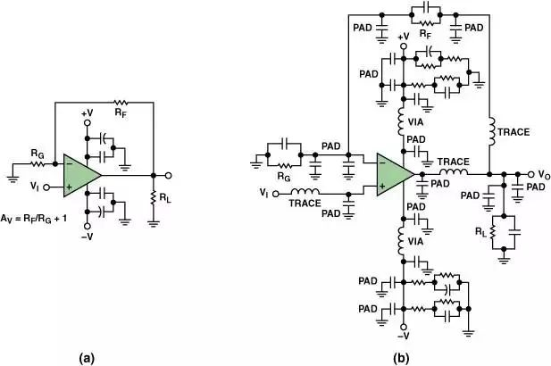 Figure 3 Typical op-amp circuit: (a) Original schematic; (b) Equivalent circuit considering parasitic effects
In high-speed circuits, even tiny parasitic parameters can degrade performance. A capacitance of only tens of picofarads (pF) is enough to cause adverse effects. For example, an extra 1 pF parasitic capacitance at the inverting input will generate a nearly 2 dB resonant peak in the frequency domain. Excessively large parasitic capacitance will further lead to circuit instability and oscillation.
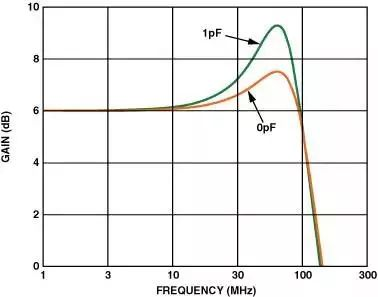 Figure 4 Resonant peak caused by parasitic capacitance
Basic formulas for calculating typical parasitic parameters are provided below for troubleshooting:
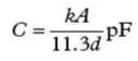
Formula (1) Parallel Plate Capacitance
Where:
C = Capacitance value
A = Area of electrode plates (unit: cm²)
k = Relative permittivity of PCB dielectric material
d = Spacing between two plates (unit: cm)
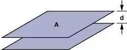 Figure 5 Capacitance between two parallel plates
Formula (2) Trace Inductance
Trace inductance is another common parasitic effect, caused by overlong traces or insufficient ground plane coverage.
Where:
W = Trace width
L = Trace length
H = Trace thickness
All dimensions are in millimeters (mm).
 Figure 6 Schematic of trace inductance
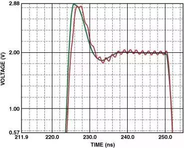
Figure 7 shows the impact of a 2.54 cm long trace at the non-inverting input of a high-speed op-amp. The equivalent parasitic inductance is 29 nH, which can trigger continuous low-amplitude oscillation throughout the transient response period. The figure also illustrates how ground planes suppress parasitic inductance.
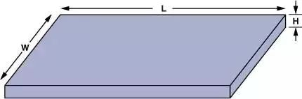 Figure 7 Pulse response with and without ground plane
Via Parasitic Parameters
Vias are another major source of parasitic inductance and capacitance.
Formula (3) Via Parasitic Inductance
Where:
T = PCB thickness
d = Via diameter (unit: cm)
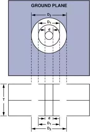 Figure 8 Dimensional parameters of a via
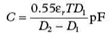
Formula (4) Via Parasitic Capacitance
Where:
\(\varepsilon_r\) = Relative permittivity of PCB material
T = PCB thickness
\(D_1\) = Pad diameter around the via
\(D_2\) = Diameter of clearance hole in the ground plane
All dimensions are in centimeters (cm).
A single via on a 0.157 cm thick PCB introduces approximately 1.2 nH parasitic inductance and 0.5 pF parasitic capacitance. This explains why designers must take strict precautions during routing to minimize parasitic effects.
Ground Planes
This section covers core characteristics of ground planes, and further research is recommended for in-depth study.
A ground plane acts as a common reference voltage, electromagnetic shield, and heat dissipation path. It reduces parasitic inductance but may increase parasitic capacitance. Despite its numerous advantages, proper implementation is required due to inherent limitations.
Ideally, dedicate one full PCB layer exclusively as the ground plane. An intact ground plane delivers optimal performance. Never occupy areas of the dedicated ground layer for other signal connections. A complete ground plane eliminates magnetic fields between conductors and ground, thus reducing trace inductance. Any break in the ground plane will introduce unexpected parasitic inductance to traces above or below it.
Thanks to its large cross-sectional area, a ground plane maintains extremely low DC resistance. Current follows the path of minimum resistance at low frequencies, while taking the path of minimum impedance at high frequencies.
In some cases, segmented ground planes perform better. Removing the ground plane beneath input and output pads can optimize the performance of high-speed op-amps. Parasitic capacitance introduced by ground planes at the input side increases the op-amp input capacitance, reduces phase margin and causes instability. As mentioned in the parasitic effect section, merely 1 pF capacitance at the op-amp input can generate obvious resonant peaks. Capacitive loads (including parasitic capacitance) at the output create additional poles in the feedback loop, which also reduce phase margin and lead to circuit instability.
Separate analog and digital circuits, along with their respective ground planes, whenever possible. Fast rising edges generate current spikes on ground planes, and the resulting noise will degrade analog performance. Connect analog ground and digital ground (as well as power supplies) to a single common ground point to suppress circulating ground current and coupled noise.
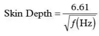
At high frequencies, the skin effect occurs: current concentrates on the outer surface of conductors, which effectively reduces the conductive cross-section and increases DC resistance. The following approximate formula calculates the skin depth of copper conductors (unit: cm):
Electroplated materials with low conductivity can mitigate the skin effect.
Routing and Shielding
PCBs carry various analog and digital signals with different voltage/current levels, ranging from DC to GHz frequencies. Isolating these signals from mutual interference is a major challenge.
As recommended earlier, make a comprehensive signal routing plan in advance. Identify sensitive signals and formulate targeted integrity protection measures. Ground planes serve as both voltage reference and shielding barriers. Physical spacing between traces is the first choice for signal isolation. Key practical guidelines are summarized as follows:
- Shorten long parallel traces and reduce coupling distance to suppress inductive crosstalk.
- Minimize the length of long traces on adjacent layers to avoid capacitive coupling.
- Route signals requiring high isolation on different layers. If complete separation is impossible, adopt orthogonal routing and place a ground plane between traces. Orthogonal routing minimizes capacitive coupling, and the intermediate ground plane provides effective electromagnetic shielding. This method is widely used for controlled-impedance traces.
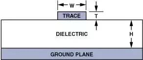
High-frequency RF signals are generally transmitted on controlled-impedance traces with fixed characteristic impedance (e.g. 50 Ω for typical RF applications). The two most common types are microstrips and striplines, implemented with different structures.
Microstrip Controlled-Impedance Trace
A microstrip can be arranged on any outer layer of a PCB, using the underlying ground plane as the reference layer.
Figure 13 Schematic of microstrip transmission line
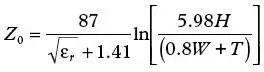
Formula (6) Characteristic Impedance of Microstrip (FR4 Material)
Where:
H = Distance between signal trace and ground plane
W = Trace width
T = Trace thickness
All dimensions are in mils (
\(10^{-3}\) inch);
\(\varepsilon_r\) = Relative permittivity of PCB material.
Stripline Controlled-Impedance Trace
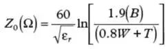
A stripline is sandwiched between two ground planes. This structure requires more PCB layers, is sensitive to dielectric thickness variation and involves higher cost, so it is only used for high-demanding applications.
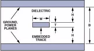 Figure 14 Schematic of stripline transmission line
Formula (7) Characteristic Impedance of Stripline
Guard Ring
A guard ring is another widely used shielding technique for op-amps, which prevents parasitic current from flowing into sensitive nodes. Its working principle is straightforward: surround the sensitive node with a continuous guard trace, and keep the guard trace at the same potential (low impedance) as the sensitive node, so as to divert parasitic current away.
Figure 15(a) shows guard ring topologies for inverting and non-inverting op-amp circuits. Figure 15(b) presents typical guard ring routing for SOT-23-5 packages.
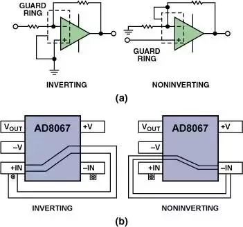 Figure 15 Guard ring: (a) Topology for inverting and non-inverting operation; (b) Routing for SOT-23-5 package
More routing and shielding techniques are available. Refer to relevant technical documents for further study.
Conclusion
Professional PCB routing is critical to the success of op-amp circuit design, especially for high-speed applications. A high-quality schematic is the foundation of reliable routing, and close collaboration between circuit designers and layout engineers (especially for component and trace placement) is essential. Key design considerations include power supply bypassing, parasitic effect suppression, ground plane layout, package influence, routing and shielding strategies.
Core PCB Design Guidelines for Op-Amp Circuits
- Place bypass and filter capacitors near chip power pins during PCB design, with a typical spacing less than 3 mm.
- Small ceramic bypass capacitors at op-amp power pins provide transient energy for high-frequency operation. Select capacitance values according to input signal frequency and op-amp speed. For a 400 MHz op-amp, a parallel combination of 0.01 µF and 1 nF capacitors is recommended.
- Pay attention to the self-resonant frequency when selecting capacitors. Capacitors whose self-resonant frequency deviates greatly from the operating frequency (e.g. 400 MHz) cannot work effectively.
- Avoid routing other traces beneath op-amp input/output pins and feedback resistors to reduce mutual parasitic capacitance and enhance circuit stability.
- Surface Mount Devices (SMDs) feature superior high-frequency performance and compact size.
- Keep PCB traces as short as possible, and optimize trace width and aspect ratio to minimize parasitic effects.
- Power traces suffer from severe parasitic DC resistance and self-inductance, so widen power traces as much as possible.
- The current on op-amp input and output interconnects is extremely small, making these traces highly vulnerable to parasitic interference.
- For signal paths longer than 1 cm, adopt controlled-impedance transmission lines with terminating resistors at both ends.
- When an op-amp drives RC loads, connect a series output resistor (\(R_{OUT}\)) close to the op-amp to isolate capacitive loads and resolve stability issues.
About Maxipcb
Maxipcb empowers innovators to turn cutting-edge technologies into reality.
We offer one-stop solutions for design, simulation, testing, PCB manufacturing, component procurement and SMT assembly, enabling efficient development, rapid deployment and risk control across the full product lifecycle.Serving the world in communications, industrial automation, aerospace, automotive, semiconductor and beyond, we build a safer, more connected future together.