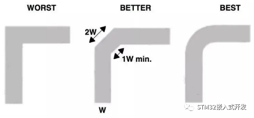
Nowadays, nearly all official PCB Layout Guides released by SoC manufacturers specify the bend angle rules for high-speed traces. It is clearly stated that high-speed signals shall not use 90° bends, and 45° bends are the preferred solution. Meanwhile, arc bends are considered to deliver better performance than 45° bends.
Nowadays, nearly all official PCB Layout Guides released by SoC manufacturers specify the bend angle rules for high-speed traces. It is clearly stated that high-speed signals shall not use 90° bends, and 45° bends are the preferred solution. Meanwhile, arc bends are considered to deliver better performance than 45° bends.
Is this statement fully accurate? How should we set the bend angle for PCB traces? Which option is better, 45° bends or arc bends? Are 90° right-angle bends completely unacceptable?
Discussions over PCB trace bend angles have only become prevalent in the past two decades. In the early 1990s, Intel, the industry leader in PC hardware at that time, led the formulation of the PCI bus specification, marking the advent of the era of high-speed system design.
Driven by Moore's Law, electronic design and IC manufacturing technologies have advanced continuously. As semiconductor process technologies are upgraded, the switching speed of transistors inside ICs keeps increasing, and the clock frequency of various buses also rises steadily. Consequently, signal integrity issues have attracted extensive research and attention across the industry.
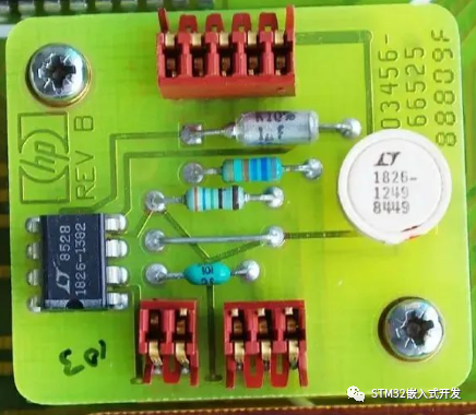
In the early days, PCB layout work was relatively straightforward. Designers only needed to route traces smoothly and keep the layout neat and aesthetic, with no need to concern about signal integrity. For instance, the PCB of the classic HP3456A multimeter shown below features a large number of 90° traces, which were intentionally routed at right angles, and copper area filling is rarely applied on the board.
In the upper-right area of the above PCB, traces are not only routed with right-angle bends but also narrowed after turning. This change in trace width will trigger signal reflection and impair signal integrity.
This article focuses on bend angle design for high-frequency and high-speed traces. We will analyze the advantages and disadvantages of traces with acute angles, right angles, obtuse angles, arcs and other arbitrary bend configurations one by one.
Why Acute-Angle Traces Are Prohibited on PCBs
Acute-angle routing is strictly forbidden in PCB design. Regardless of its impact on high-speed signal transmission, acute bends must be avoided from the perspective of Design for Manufacturability (DFM).
Acute intersections between PCB traces will form so-called acid traps. During the PCB etching process, copper foils at acid trap areas will be over-etched, which may result in intermittent open circuits on traces.
Tools such as CAM 350 can perform automated DFM audits to detect potential acid trap risks in advance and eliminate manufacturing bottlenecks. If fabricators identify acid traps on finished PCB files, they will simply add copper patches to fill the gaps.
Most process engineers at PCB factories only handle issues from a manufacturing perspective and lack professional layout knowledge. Their remedial measures for acid traps may introduce new signal integrity risks. Therefore, we should avoid generating acid traps at the source during layout design.
Methods to Avoid Acid Traps Caused by Acute-Angle Routing
Modern EDA software including Cadence Allegro and Altium Designer are equipped with comprehensive routing auxiliary functions. Proper use of these features can effectively prevent acid traps.
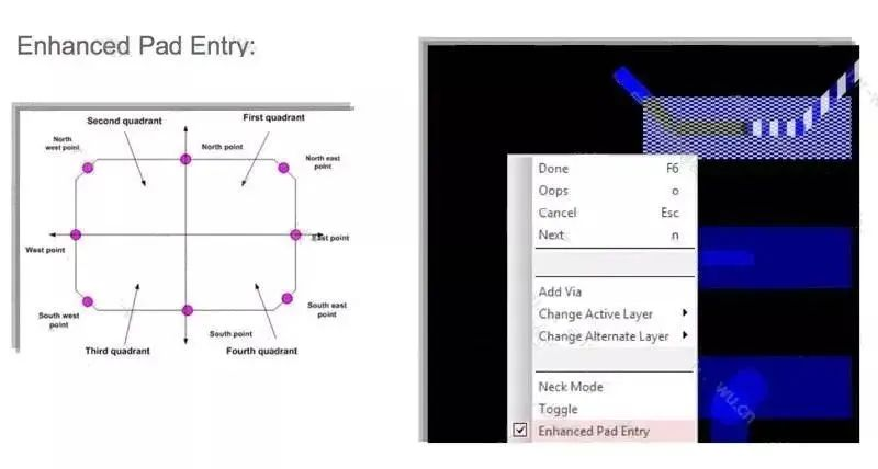
- Optimize trace exit angles from pads to avoid acute angles between traces and pads, as shown in the figure below.
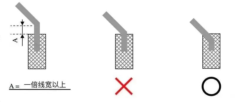
The
Enhanced Pad Entry function in Cadence Allegro helps eliminate acute angles at pad outlets and prevent acid trap-related DFM issues.
-
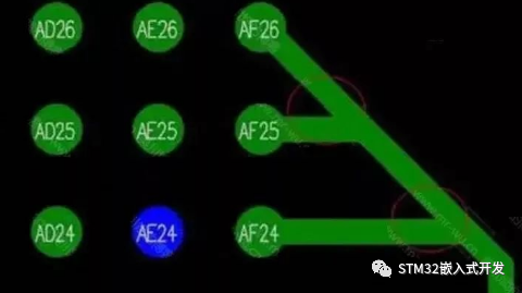
Prevent acute angles formed by the intersection of two independent traces.
-
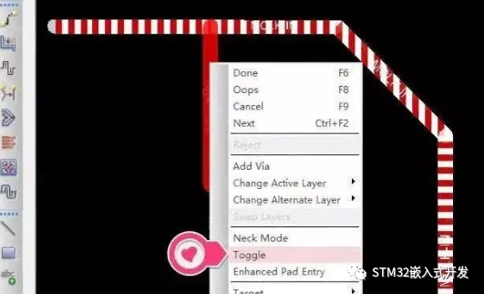
Use the routing toggle function in Cadence Allegro to avoid acute angles at T-junctions of traces, so as to rule out acid trap risks.
Is 90° Routing Allowed in PCB Layout?
Nearly all official PCB design guidelines require designers to avoid 90° bends for high-frequency and high-speed traces. High-speed transmission lines require consistent characteristic impedance, while a 90° bend will cause local widening of the trace. The effective width at a 90° bend is approximately 1.414 times the standard trace width, leading to signal reflection.
In addition, extra parasitic capacitance generated at right-angle bends will introduce additional propagation delay to signals.
Signals propagate without reflection or distortion on uniform transmission lines. Once a 90° bend exists, the trace width will change locally. According to electromagnetic field theories, such discontinuity will inevitably cause signal reflection.
The adverse effects of 90° bends on signals are mainly reflected in three aspects:
- A right-angle bend acts as a capacitive load on the transmission line and slows down the signal rise time.
- The expanded trace width at 90° bends causes impedance discontinuity and further induces signal reflection.
- Sharp corners of right-angle bends are prone to radiate or receive electromagnetic waves, resulting in electromagnetic interference (EMI).
The parasitic capacitance of a right-angle bend on a transmission line can be calculated via the empirical formula below:
\(C=61W\sqrt{E_r}/Z_O\)
Where:
C = Equivalent capacitance of the bend (unit: pF)
W = Standard trace width (unit: inch)
\(E_r\) = Relative permittivity of dielectric material
\(Z_O\) = Characteristic impedance of the transmission line
For conventional high-speed digital PCBs with dense routing, the typical trace width is 4~5 mil. A single 90° bend produces a parasitic capacitance of roughly 10 fF, which brings a total delay of about 0.25 ps. For digital signals with a 100 ps rise time, such a 90° bend will not cause obvious performance degradation.
For high-frequency signal lines, wider traces are usually adopted to mitigate damage caused by the skin effect. Taking a 50 Ω transmission line with a 100 mil standard width as an example, the effective width at a 90° bend reaches 141 mil, and the corresponding parasitic capacitance introduces a delay of around 25 ps. In this case, 90° bends will severely impair signal quality.
Microwave transmission lines require minimal signal loss. Impedance discontinuity and extra parasitic capacitance at 90° bends will trigger phase shift and amplitude error of high-frequency signals, mismatch between input and output ports, and unintended parasitic coupling. These problems will degrade overall circuit performance and deteriorate the transmission characteristics of PCB traces.
In summary, it is strongly recommended to avoid 90° bends in PCB routing.
45° Chamfered Traces
Except for RF signals and other special-purpose signals, 45° bends are the preferred choice for general PCB traces.
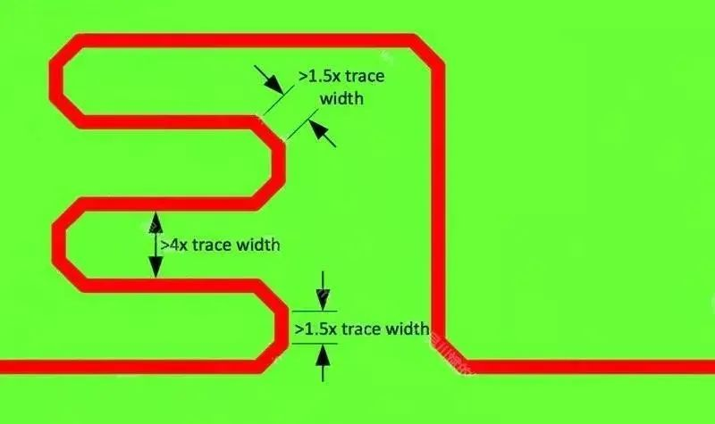
For length matching routing with 45° bends, two key rules shall be followed:
- The length of the 45° bend segment shall be no less than 1.5 times the trace width;
- The spacing between adjacent length-matching traces shall be no less than 4 times the trace width.
High-speed signals always propagate along paths with matched impedance. If the gap between length-matching traces is too narrow, inter-trace parasitic capacitance will cause signals to take shortcuts and result in inaccurate length matching. Modern EDA software supports one-click configuration of relevant routing constraints.
Arc Traces
Arc routing is not mandatory for common designs unless specified by technical specifications or applied to RF/microwave transmission lines. In high-speed and high-density PCB layout, a large number of arc traces will complicate subsequent trace modification and occupy excessive board space.
Nevertheless, arc bends are recommended for high-speed differential signals such as USB 3.1 and HDMI 2.0. For RF and microwave transmission lines, arc bends, or even 45° chamfered bends, are the optimal solutions.
Conclusion
With the development of 4G/5G wireless communication and iterative upgrading of electronic products, the data transmission rate of mainstream PCB interfaces has exceeded 10 Gbps or even 25 Gbps, and the speed is still growing rapidly. Higher requirements for PCB impedance control and signal integrity have been put forward accordingly.
For digital signals on PCBs, dielectric materials such as FR4 are regarded as homogeneous media for low-speed and low-frequency applications. However, when the signal rate on system buses reaches the Gbps level, this assumption no longer holds. Gaps between glass fiber bundles inside the epoxy substrate will cause local fluctuations of the dielectric constant. Such variations will make trace delay and characteristic impedance position-dependent and interfere with high-speed signal transmission.
Test results based on FR4 substrates show that the relative position between microstrip lines and glass fiber bundles leads to obvious fluctuation of the effective dielectric constant of transmission lines, with a maximum deviation of \(\Delta\varepsilon_r=0.4\). Although the deviation seems minor, it will severely affect differential transmission lines operating at 5~10 Gbps.
To suppress the impact of the fiber weave effect in high-speed design projects, zig-zag routing is an effective solution.
Cadence Allegro PCB Editor 16.6-2015 and later versions support the zig-zag routing function. Users can enable this feature via the menu path: Route -> Unsupported Prototype -> Fiber Weave Effect.
Twenty years ago, PCB designers did not need to consider arc routing or the fiber weave effect on high-speed signals.
PCB layout rules are not static. As PCB manufacturing processes and data transmission speeds continue to improve, some currently applicable rules may become obsolete in the future.
About Maxipcb
Maxipcb empowers innovators to turn cutting-edge technologies into reality.
We offer one-stop solutions for design, simulation, testing, PCB manufacturing, component procurement and SMT assembly, enabling efficient development, rapid deployment and risk control across the full product lifecycle.Serving the world in communications, industrial automation, aerospace, automotive, semiconductor and beyond, we build a safer, more connected future together.