In most electronic systems, noise reduction is a core design requirement. Just like power consumption limits, ambient temperature variation, dimensional constraints, speed and accuracy specifications, the pervasive noise must be properly managed to ensure successful product design.
In most electronic systems, noise reduction is a core design requirement. Just like power consumption limits, ambient temperature variation, dimensional constraints, speed and accuracy specifications, the pervasive noise must be properly managed to ensure successful product design.
This article does not elaborate on solutions for suppressing external noise (noise entering the system along with signals), as such interference is generally beyond the direct control of design engineers. In contrast, preventing internal noise — noise generated or coupled inside circuits and systems — from corrupting valid signals is an essential responsibility of design engineers. Today we focus on grounding design, with emphasis on grounding techniques for high-frequency circuits.
Grounding generally refers to connecting circuits, equipment or systems to a high-conductivity conductor that acts as a reference potential point or plane, so as to create a low-impedance path between the circuit/system and ground.
A ground line serves as an equipotential reference for circuit potential and acts as the common conductor for all circuits in a system. Current of every circuit flows back through ground lines to form complete loops. However, all conductors have inherent impedance. When current passes through a ground line, a voltage drop will be generated in accordance with Ohm’s Law, which means the ground line cannot remain an ideal equipotential body. Therefore, the assumption that all points on a ground line share the same potential is invalid in practical design. In fact, potential differences exist between different positions on ground lines, and such differences can be quite significant in some cases. The common impedance of ground lines causes voltage deviations among grounding points, which further induces ground interference.
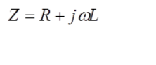
As mentioned above, a ground line, as a conductor, has inherent impedance consisting of resistance and inductive reactance.
Conductor impedance is a function of frequency and rises sharply as frequency increases. High-speed digital circuits operate at high clock frequencies, and pulse signals contain abundant high-frequency components. This will produce considerable voltage on ground lines, making ground impedance a prominent interference source for digital circuits.
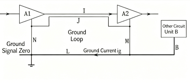
In PCB design for electronic products, suppressing ground interference is one of the top priorities. Interference always occurs between different circuit units, modules or systems. Ground interference refers to signal interference transmitted via shared ground lines. Note that the signals discussed herein mainly refer to AC signals or transient switching signals. Ground interference falls into three categories: ground loop interference, electromagnetic coupling interference of ground loops, and common impedance interference. The figure below clearly illustrates the formation mechanisms of the three types of ground interference.
1. Ground Loop Interference
Different currents flow through individual conductors horizontally, generating differential-mode voltages that affect circuit operation. Specifically, the ground current of Circuit Unit B flows through the ground loop formed by nodes J, N, L and M, and interferes with Amplifier A1 and A2. This type of interference is named ground loop interference because it is induced by loop current formed by cables and ground lines.
2. Electromagnetic Coupling Interference of Ground Loops
On actual PCBs, the ground loop enclosed by J, N, L and M occupies a certain physical area. According to the law of electromagnetic induction, a varying magnetic field within this enclosed area will induce current in the loop and cause interference. Time-varying magnetic fields exist ubiquitously in the surrounding environment, so a larger loop area will lead to more severe interference.
3. Common Impedance Interference
Analyze the circuit structure in the above figure. One connection among J, N, L and M is redundant. Removing any one of them can keep all grounding points connected and eliminate the ground loop. The selection of the redundant connection to remove needs to take another interference type — common impedance interference — into account.
① Remove J: This is the worst solution. Although the original ground loop is eliminated, a new loop composed of signal line I, N, L and M is formed, which brings more severe interference than the original structure.
② Remove M: The ground loop disappears. However, the ground current of Amplifier A2 has to flow through J and N to the ground reference point. Since segment N is the shared ground line for both A1 and A2, the voltage drop generated by A2’s ground current on N will be superimposed on A1 and cause interference. Interference caused by shared ground segments is defined as
common impedance interference.
③ Remove L: This method fails to solve the common impedance issue between A1 and A2, and additionally introduces common impedance interference between Circuit Unit B and the two amplifiers.
④ Remove N: This is a relatively feasible option. Even so, segment M becomes the shared impedance for A1 and A2, which still generates interference. Nevertheless, the interference is transmitted from the preceding-stage A1 to the subsequent-stage A2. Since the signal amplitude of A2 is much higher than that of A1, the interference from A1 will hardly cause adverse impacts.
The most reasonable routing scheme is to remove connection N and connect the bottom end of M directly to the ground reference point.
The above content explains the generation mechanisms of ground interference. The following introduces four mainstream grounding methods. Combined with the above principles, designers can select the optimal low-interference grounding scheme in practical PCB design and develop reliable circuits and systems.
Signal grounding methods are mainly divided into four types: single-point grounding, multi-point grounding, hybrid grounding and floating grounding.
1. Single-Point Grounding
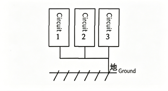
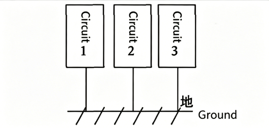
Single-point grounding means designating one node in the entire system as the ground reference. All ground lines of circuits and equipment are connected to this node, which serves as the zero-potential reference for the whole system. Single-point grounding is further classified into series single-point grounding and parallel single-point grounding.
Figure 2 Series Single-Point Grounding
For series single-point grounding, high-power circuits produce large return current. A voltage drop will occur across the finite impedance of ground lines, resulting in potential deviation between circuits and the reference ground. This may cause the system to operate abnormally. This method is not applicable to systems with circuits of different power ratings, because large return current from high-power circuits will interfere with low-power circuits and components. If series single-point grounding has to be adopted, place the most sensitive circuits near the power input terminal and keep them far away from low-power devices.
Series single-point grounding features simple structure and routing. The overall ground impedance remains low if the ground leads of each circuit are short. It can be adopted when the potential difference between grounding nodes of different circuits is insignificant.
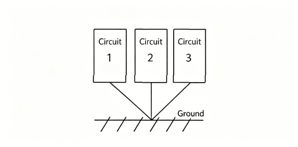 Figure 3 Parallel Single-Point Grounding
In parallel single-point grounding, each circuit unit uses an independent ground line connected to the unified reference node. Its advantage is that the potential of each grounding node is only affected by the local ground current and ground impedance, free from interference from other circuits. This method can effectively suppress low-impedance crosstalk between circuit units at low frequencies, yet it also has obvious drawbacks. Firstly, numerous independent ground lines are required, which increases total ground line length and corresponding impedance, leading to complex layout and poor practicability. Secondly, mutual coupling will occur between parallel ground lines. As frequency rises, the impedance, inductance and capacitance of ground lines all increase rapidly. Therefore, parallel single-point grounding is not suitable for high-frequency circuits.
2. Multi-Point Grounding
Multi-point grounding means all circuits and components requiring grounding in a system are connected directly to the nearest ground plane. This minimizes the length of ground leads and reduces ground impedance to the lowest level.
When the operating frequency of an electronic system exceeds 1 MHz and the signal wavelength is comparable to the length of ground leads, the ground line behaves like a short-circuited transmission line with standing waves of current and voltage distributed along it. In this case, the ground line turns into a radiating antenna and loses its basic grounding function. To reduce ground impedance and suppress radiation, the length of ground leads shall be less than 1/20 of the signal wavelength. For this reason, single-point grounding is no longer feasible, and multi-point grounding becomes the preferred solution.
Multi-point grounding features simple circuit structure and greatly suppresses high-frequency standing waves on ground lines. However, it may form numerous internal ground loops within equipment and weaken the immunity to external electromagnetic fields. Special attention shall be paid to ground loop issues, especially when interconnecting different modules and devices with multi-point grounding.
In general, single-point grounding is recommended for frequencies below 1 MHz, multi-point grounding for frequencies above 10 MHz, and hybrid grounding for the frequency range of 1 MHz ~ 10 MHz.
3. Hybrid Grounding
Hybrid grounding combines the characteristics of single-point grounding and multi-point grounding, and is widely used on PCBs with mixed low-frequency and high-frequency signals.
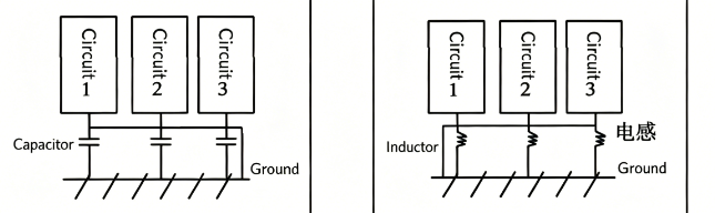 Figure 5 Hybrid Grounding (Capacitive Coupling)
Figure 6 Hybrid Grounding (Inductive Coupling)
Two typical hybrid grounding topologies are shown in Figure 5 and Figure 6. The capacitive coupling topology operates as single-point grounding at low frequencies and switches to multi-point grounding at high frequencies, since capacitors shunt high-frequency current to ground. The key to applying this method is to clarify the operating frequency range and the expected flow direction of ground current.
Capacitors and inductors deployed in grounding topologies enable designers to control radio frequency (RF) current paths in an optimized way. Defining RF current loops properly guides reasonable PCB routing. Inadequate understanding of RF return paths will lead to electromagnetic radiation or susceptibility issues.
4. Floating Grounding
Floating grounding means the internal grounding system of equipment is electrically isolated from the chassis earth connection, so as to prevent electromagnetic interference from the chassis from coupling into the equipment. Nevertheless, since the equipment is not connected to the common ground, static charge tends to accumulate between the two isolated systems. When the potential difference rises to a certain level, intense electrostatic discharge (ESD) will occur and generate interference current. Floating grounding is not applicable to communication systems.
Based on the above theories, reasonable ground layout shall be implemented in actual PCB design. The key guidelines for ground layout are summarized as follows:
- Separate digital ground and analog ground;
- Avoid forming closed loops for digital circuit ground lines;
- In multi-layer PCBs, arrange ground layers and power layers as adjacent layers whenever possible;
- Optimize the width of ground lines, power lines and signal traces.
Practical experience and continuous exploration are required to fully apply the above guidelines.
For high-speed circuit design, proper grounding is one of the most effective Electromagnetic Compatibility (EMC) design techniques. Statistics show that 90% of EMC problems are caused by improper routing and grounding. Well-designed routing and grounding can enhance circuit immunity, reduce electromagnetic emission, and resolve most electromagnetic interference issues at low cost. Therefore, rational grounding design is critical for high-speed PCB development.
It is generally recommended that power and signal current return through dedicated ground planes, which also serve as reference nodes for converters, voltage references and other sub-circuits. However, even full adoption of ground planes cannot guarantee high-quality ground reference for AC circuits.
Figure 1 shows a two-layer PCB design with a simple circuit. An AC/DC current source is placed on the top layer, with one terminal connected to Via 1 and the other terminal connected to Via 2 via a U-shaped copper trace. Both vias penetrate the PCB and connect to the ground plane. In an ideal state with zero impedance, the voltage across the current source is 0 V.
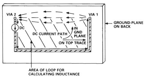 Figure 1 Schematic and layout of current source: U-shaped trace on PCB with current returning via ground plane
The simplified schematic cannot reflect real operating conditions. Analyzing how current flows from Via 1 to Via 2 on the ground plane helps identify practical problems and develop solutions to eliminate high-frequency ground noise caused by improper layout.
Inductance is proportional to the area of the current loop, which can be explained by the right-hand rule and magnetic field distribution shown in Figure 2. Magnetic fields generated by current flowing along all segments inside a loop reinforce each other, while fields outside the loop cancel each other out. Therefore, magnetic fields are mainly confined within the loop. A larger loop area means higher inductance, which results in greater magnetic energy storage, higher impedance and larger voltage drop at a given frequency.
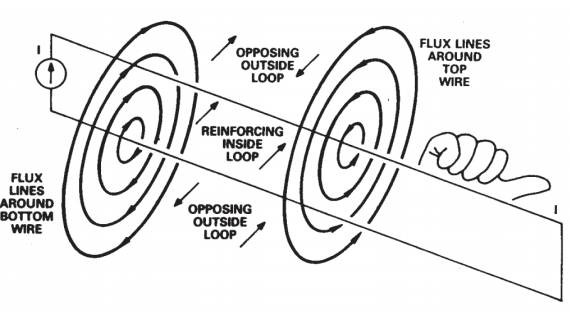 Figure 2 Magnetic field lines and inductive loop
In the above example, the loop with the minimum area is formed by the U-shaped top trace and the corresponding area of the ground plane directly underneath. Figure 3 (left) illustrates the primary return path of AC current on the ground plane, which is directly below the U-shaped trace and forms the smallest loop. In practical scenarios, the resistance of the ground plane causes low-to-medium frequency current to flow through a path between the direct return route and the area right below the top trace (Figure 3 right). Even for frequencies as low as 1~2 MHz, the return path remains close to the upper trace.
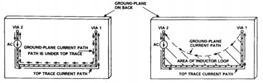 Figure 3 AC current return paths on ground plane: (Left) Ideal path without ground plane resistance; (Right) Actual path with ground plane resistance
Layout Troubleshooting
Once the current return paths on ground planes are clarified, common layout defects can be identified and corrected. For the layout shown in Figure 4, Path A is defined as a critical high-speed path. It shall be kept as short as possible, routed away from digital traces, and free of vias. Path B is non-critical but needs to cross Path A. A common practice is to cut an opening on the ground plane beneath Path A, then route Path B through two vias under Path A.
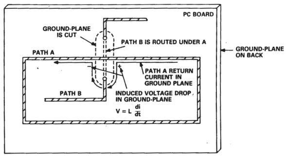 Figure 4 Typical PCB layout issue for intersecting signal paths
This solution leads to adverse consequences: the cut on the ground plane enlarges the area of both current loops and introduces extra inductance to the ground return paths of the two signals. Since Path A carries high-frequency signals, an obvious voltage drop will occur across the ground plane opening. For typical ECL or TTL signals, this voltage drop can reach hundreds of millivolts, which severely degrades the performance of 12-bit 10 MHz converters and 8-bit 20 MHz converters. A simple remedy is to add a jumper wire across the ground plane opening to maintain a small loop area.
Power supply interference is another key concern. Power lines shall be designed with the lowest possible characteristic impedance. To achieve this, place the ground plane directly underneath power lines to reduce inductance and increase distributed capacitance. Deploy bypass capacitors at key positions to further boost capacitance. If only capacitance is considered — for instance, mounting a 0.1 µF capacitor at power pins to lower impedance — a power line with 30 nH inductance will generate approximately 3 MHz damped oscillation after each transient switching.
About Maxipcb
Maxipcb empowers innovators to turn cutting-edge technologies into reality.
We offer one-stop solutions for design, simulation, testing, PCB manufacturing, component procurement and SMT assembly, enabling efficient development, rapid deployment and risk control across the full product lifecycle.Serving the world in communications, industrial automation, aerospace, automotive, semiconductor and beyond, we build a safer, more connected future together.