This article will explore seven essential (and critical) tips and strategies applicable to both novice and experienced PCB designers. By paying attention to these tips throughout the design process, you and your team can reduce the number of design iterations, shorten design time, and lighten the diagnostic workload for the final design results. Let us examine them one by one.
This article will explore seven essential (and critical) tips and strategies applicable to both novice and experienced PCB designers. By paying attention to these tips throughout the design process, you and your team can reduce the number of design iterations, shorten design time, and lighten the diagnostic workload for the final design results. Let us examine them one by one.
1. Be Familiar with the Factory Manufacturing Process
In this era of fabless IC companies, many engineers are not really familiar with the PCB manufacturing steps and chemical processes involved in producing boards from their design files – and that is not surprising. However, this lack of practical knowledge often leads novice engineers to make unnecessarily complex design decisions.
Does the design really need to be that complex? Could a larger routing grid be used to reduce board cost and improve reliability? Other common mistakes made by novices include unnecessarily small via sizes and unnecessary use of blind and buried vias. Those advanced via structures are powerful tools for PCB designers, but their effectiveness is highly context‑dependent. Just because they are available does not mean they must be used.
In one blog post, PCB design expert Bert Simonovich discussed via aspect ratio: "A 6:1 aspect ratio for vias will ensure that your board can be manufactured anywhere." With a little thought and planning, most designs can avoid high‑density interconnect (HDI) features, saving cost and improving manufacturability.
Not all PCB foundries are equally adept at the physics and fluid mechanics required for copper plating of ultra‑small or dead‑ended vias. Remember, a single bad via can ruin an entire board; if your design has 20,000 vias, you have 20,000 opportunities for failure. Unnecessarily using HDI vias can immediately send the failure rate skyrocketing.
2. Schematics Simplify the Design Task
Sometimes, for a simple board design, drawing a schematic seems like a waste of time – especially if you already have one or two designs under your belt. However, for first‑time PCB designers, drawing a schematic can also be a daunting task. Skipping the schematic is a strategy sometimes adopted by novices and moderately experienced design engineers. However, starting with a complete schematic that can serve as a reference helps ensure that all your routing connections are completed. Here is why.
First, the schematic is a visual representation of the PCB circuit, conveying multiple layers of information. Sub‑circuits are drawn in detail across several pages, and components with corresponding functions can be placed near each other, regardless of their final physical layout. Second, because schematic symbols label every pin of each component, it is easy to check for unconnected pins. In other words, regardless of whether formal rules are followed, the schematic helps you quickly visually verify circuit completeness.
Having a schematic as a template when designing a PCB simplifies the routing task. By using schematic symbols to complete connections, you can tackle routing challenges without constantly second‑guessing connections. In the end, you will save a design re‑spin by catching a trace connection that would otherwise be missed in the first revision.
3. Use an Auto‑Router but Don't Rely on It
Most professional PCB CAD tools include an auto‑router. However, unless you are a professional PCB designer, an auto‑router is at best a tool for getting the design through an initial pass. It is not a one‑click solution for PCB circuit connections – you still need to know how to route manually.
An auto‑router is a highly configurable tool. To get the most out of it, the router parameters must be carefully and thoroughly set up for each task, and even for individual modules on a single PCB. In short, there is no one‑size‑fits‑all default.
When you ask an experienced design engineer, "Which auto‑router is best?" they will answer, "The one between your ears" – and they mean it. Routing is as much an art as it is an algorithmic process; it is inherently heuristic, similar to traditional backtracking algorithms.
Backtracking algorithms are well‑suited for finding solutions in constrained search spaces, such as mazes or puzzles, where path choices are limited. However, in an open, unconstrained environment such as a pre‑placed PCB, backtracking algorithms do not excel at finding optimal solutions. Unless the auto‑router constraints have been carefully fine‑tuned by the engineer, the resulting routing still requires manual inspection of the weaknesses in the backtracking results.
Trace size is another issue. The auto‑router does not know with certainty how much current you intend to pass through a given trace, so it cannot determine the appropriate trace width for you. Consequently, most auto‑routers produce traces whose widths do not meet specifications.
When considering an auto‑router, ask yourself: "How much time will I have left to manually route after setting up the router constraints for the board, and even individual trace constraints on the schematic?" Experienced design engineers spend most of their effort on initial component placement, devoting nearly half of the entire design time to optimising the layout from three perspectives:
-
Routing simplification – minimising rat's‑nest crossings, etc.
-
Component proximity – keeping routing as short as possible.
-
Signal timing considerations.
Veterans often use a hybrid approach to routing – doing critical routing manually, locking those traces in place, and then using the auto‑router for non‑critical traces. Designating auto‑routing areas helps manage the "runaway" state in the routing algorithm. This approach sometimes achieves a good compromise between the controllability of manual routing and the speed of auto‑routing.
4. Consider Board Dimensions and Current
Most people involved in electronics design know that, like a river following a channel, flowing electrons can also encounter bottlenecks and choke points. This principle is directly applied in the design of automotive fuses. By controlling trace thickness and shape (U‑bends, V‑bends, S‑bends, etc.), a fuse can be calibrated to melt at a choke point during current overload.
The problem is that design engineers occasionally encounter similar electrical choke points in their PCB designs. For example: using a 90° bend where two steep 45° bends would suffice; or when the bend exceeds 90°, using a zig‑zag shape. At best, those traces will slow signal propagation; at worst, they will act like automotive fuses and melt at the resistive point.
5. Avoid Sliver Risks
A sliver is a manufacturing defect that can be best managed through proper board design (see Figure 1). To understand the sliver problem, we need to review the chemical etching process. Chemical etching is used to dissolve unwanted copper. However, if the portions to be etched are particularly long, thin, or flaky, those shapes can sometimes peel off entirely before being completely dissolved. Such slivers can float in the chemical solution and may randomly land on another board.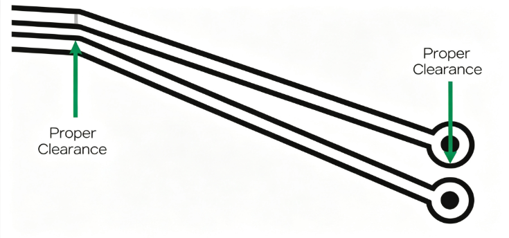
Figure 1 – In this case, the narrow shield between traces is safe for the substrate.
Another risk is that a sliver may remain on the original board. If the sliver is narrow enough, the acid bath may dissolve enough copper underneath to cause the sliver to partially lift off. The sliver then flaps like a flag, eventually falling onto the board and shorting other traces.
So, where should you look for potential slivers, and how can you avoid them? When routing, it is best to avoid leaving very narrow copper regions (as shown in Figure 2). Such areas typically occur where trace‑to‑pad clearances intersect and planes are filled (Figure 3). Setting the minimum copper width to a value greater than the manufacturer's minimum will generally keep your design free of this problem. A standard minimum etch width is 0.006 inches.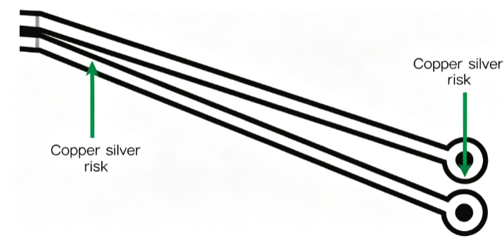
Figure 2 – A very narrow sliver risk area, such as this one in the original design file, may peel off uncontrollably during manufacturing, causing shorts and yield issues.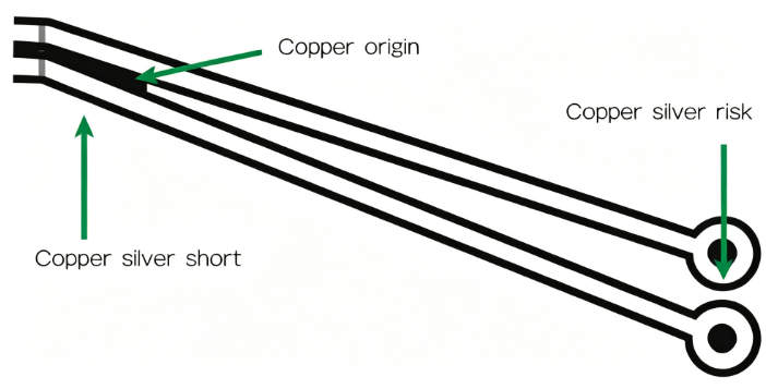
Figure 3 – In this case, chemical etching will alter the shape/size of the narrow sliver fill; when the sliver peels off, it creates unexpected debris or floating material.
6. Pay Attention to DRC
Auto‑router settings are typically aimed at design functionality, while the Design Rule Checker (DRC) is generally used to capture manufacturing design constraints. Although the setup process is similarly tedious, it is far more manageable than the auto‑router. Most design teams eventually establish a comprehensive set of design rules aimed at standardising bare‑board fabrication costs, maximising yield, and making assembly, inspection, and testing as consistent as possible.
Beyond benefiting the design itself, these design rules – by keeping the design within predefined manufacturing limits – also help create consistency in the procurement department. If board fabrication costs are consistent, procurement can often reduce the number of specific PCB manufacturing agreements that need to be maintained.
To address all these issues, many PCB design tools include built‑in DRC – some call them "constraint managers" – which interactively flag design violations as you edit. Once you set up the DRC rules for your chosen manufacturer, you need to be prepared to take the errors seriously.
DRC tools are generally conservative in their design; they can make mistakes in reporting possible errors, and it is up to you to judge. Sifting through hundreds of "possible" problems can be tedious, but it must be done. Hidden among these lists could be the reason your first tape‑out is doomed to fail. Moreover, if your design triggers a large number of potential errors, it indicates that your routing approach needs improvement.
Dave Baker, a PCB design engineer at Sunstone Circuits with over 20 years of experience, advises: "Take the time to understand and correctly set up the constraint system provided by your routing tools, and review all levels of constraints. Constraint tools can be powerful and flexible, but they can also be confusing and dangerous. Incorrect constraints can easily result in defective or un‑manufacturable boards, and errors in constraint settings are likely to limit or even disable DRC."
He gives an example: "What can happen is that every DRC passes, yet the board is still un‑manufacturable or non‑functional. I have seen this before – the design team was thrilled that the board passed DRC, only to have the first units go up in smoke on the test bench. Tracing the failure back, the team checked the CAD tool's constraint manager. The constraint manager has no design awareness – it will let you do whatever you want, no matter how bad it is."
For example, Sunstone Circuits almost daily receives requests for quotes on boards that could be easily built, except that in some critical areas, the design tolerances and clearances have been severely compressed. This forces the PCB foundry (like Sunstone) to deliver bad news: either they cannot manufacture the board because the tolerances exceed their capabilities, or they can manufacture it but with added cost and yield risks. Those customers would benefit from designing with the specific manufacturer's capabilities in mind from the start.
7. Know Your Foundry Partner
After discussing DRC setup, this final PCB design tip is almost – but not entirely – redundant. Beyond helping you set up DRC rules correctly, understanding the manufacturer that will be producing your board can provide some additional pre‑production assistance.
Good foundries will offer pre‑order assistance and advice, including how to handle your design to reduce iterations, minimise problems encountered on the test bench, and improve board production yield. Hugo, a PhD student at Carnegie Mellon University, made the following comments on understanding manufacturer issues in a blog post:
"Every manufacturer has its own specifications, such as minimum trace width, spacing, number of layers, etc. Before starting your design, you should consider your requirements and then find a manufacturer that meets them. Your requirements also include PCB material grades, from FR‑1 (paper‑phenolic resin blend) all the way to FR‑5 (fibreglass and epoxy). Most PCB prototyping manufacturers use FR‑4, but FR‑2 is also commonly used in high‑volume consumer applications. The material type affects the board's strength, durability, moisture absorption, and flame retardancy (FR)."
Understanding the PCB process – and which processes and production methods your manufacturer uses – helps you make better design decisions. Visiting your preferred manufacturing service provider to see the process in person might surprise you. Also, make good use of Design for Manufacturability (DFM) tools before sending your design to production.
Summary
If you have mastered the seven basic tips above, you are well on your way to achieving fast, reliable, professional‑quality PCBs.
Use all the design tools provided by your CAD software wisely, including auto‑placement and auto‑routing, but be patient and thorough in setting up the auto‑router to achieve good results. Do not rely on the auto‑router to do everything beyond routing; adjust trace sizes manually where necessary to ensure proper current handling. And above all, trust the rat's‑nest connections. Only when all of this is done will your circuit design succeed.
About Maxipcb
Maxipcb empowers innovators to turn cutting-edge technologies into reality.We offer one-stop solutions for design, simulation, testing, PCB manufacturing, component procurement and SMT assembly, enabling efficient development, rapid deployment and risk control across the full product lifecycle.
Serving the world in communications, industrial automation, aerospace, automotive, semiconductor and beyond, we build a safer, more connected future together.
