In PCB EMC design, layer setup comes first. The total layer count consists of power layers, ground layers, and signal layers. Besides component selection and circuit design, sound PCB layout is critical for product EMC performance.
The core of PCB EMC design is to minimize return current loops and guide return paths along intended routes. Proper layer design is the foundation for optimal EMC.
In PCB EMC design, layer setup comes first. The total layer count consists of power layers, ground layers, and signal layers. Besides component selection and circuit design, sound PCB layout is critical for product EMC performance.
The core of PCB EMC design is to minimize return current loops and guide return paths along intended routes. Proper layer design is the foundation for optimal EMC.
I. PCB Layer Design Principles
The core of PCB stack‑up planning for EMC is to properly arrange signal return paths, minimize return loop area from the board’s reference planes, and achieve flux cancellation or minimization.
1. Reference Plane (Mirror Layer)
A reference plane is a solid copper plane (power or ground) adjacent to signal layers inside the PCB. Its main functions:
- Reduce return noise: Provides a low‑impedance path for signal return currents, especially under high current in PDN.
- Lower EMI: Reduces the area of the closed loop formed by signal and return currents.
- Reduce crosstalk: Controls crosstalk between high‑speed digital traces; smaller height to reference plane = less crosstalk.
- Impedance control: Prevents signal reflection.
2. Reference Plane Selection
Both power and ground planes can serve as references and provide shielding.
- Power planes have higher characteristic impedance, large voltage deviation, and more high‑frequency noise.
- Ground planes are well‑grounded as the zero reference, offering far better shielding.
Priority: Ground plane first, power plane second.
II. Principle of Flux Cancellation
According to Maxwell’s equations, electric and magnetic interactions between charged bodies or currents propagate through the intermediate medium (vacuum or material).
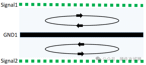
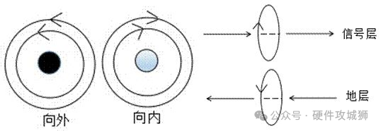
In PCBs, magnetic flux propagates along transmission lines. If the RF return path runs parallel and close to the signal path, flux from the signal and return paths flows in opposite directions and cancels each other.
III. Flux Cancellation
Flux cancellation is essentially control of the signal return path.
IV. Right‑Hand Rule
When current flows through a wire, a magnetic field forms around it, whose direction follows the right‑hand rule.
For two parallel, closely spaced wires:
- One carries signal current outward; the other carries return current inward.
- Currents are equal in magnitude and opposite in direction.
- Magnetic fields are equal and opposite, so they cancel each other.
This explains strong flux cancellation when a signal layer is adjacent to a ground plane.
V. 6‑Layer PCB Design Examples
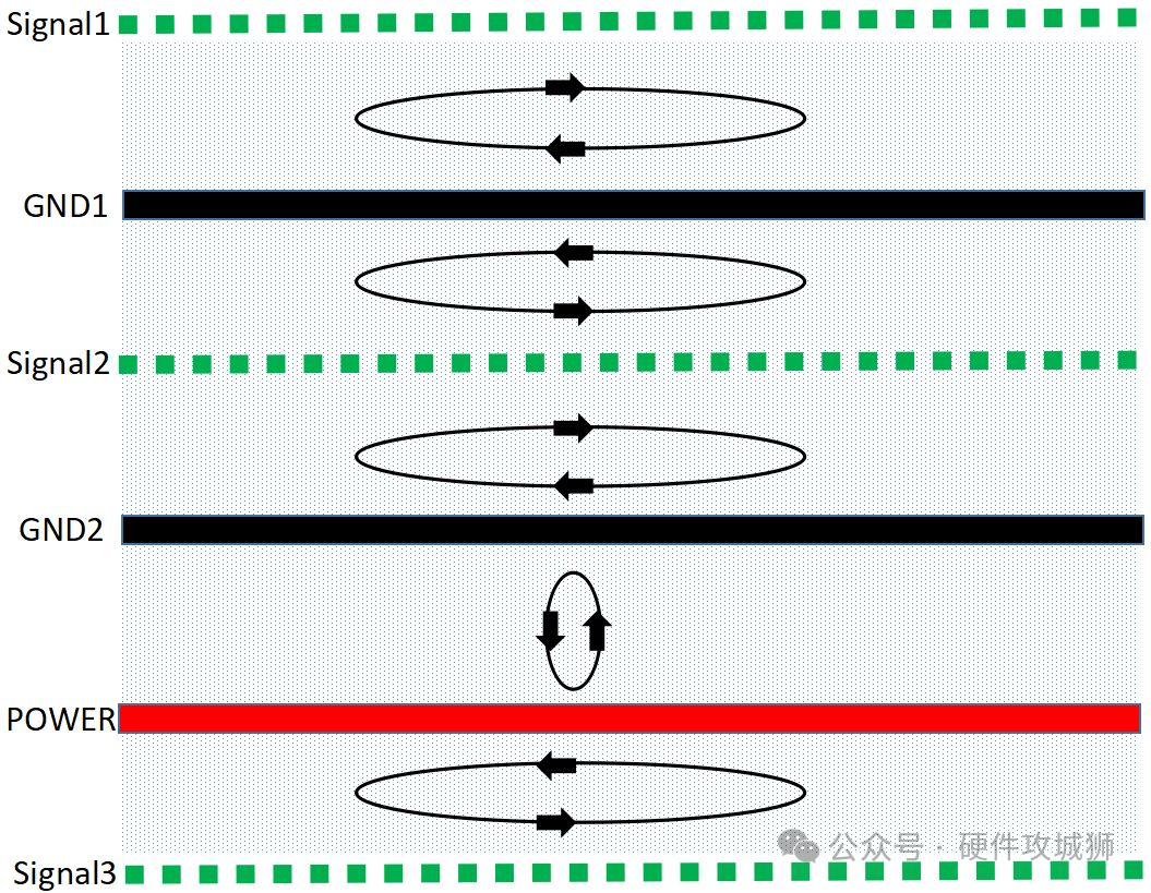
Preferred Option 3 (Best EMC)
Analysis:
- Signal layers S1, S2, S3 are adjacent to reference planes → optimal flux cancellation.
- Preferred routing layers: S2 > S3 > S1.
- Power and ground planes are adjacent with small spacing → low impedance and strong flux cancellation.
- Main power and its ground on layers 4 & 5.
- Increase S2–P spacing; reduce P–G2 (and G1–S2) spacing to lower power plane impedance and reduce interference to S2.
Option 1 (Cost‑Sensitive)
Analysis:
- S1, S2 close to ground → excellent flux cancellation.
- Power plane routes through S3, S2 to GND → poor flux cancellation and high impedance.
- Preferred routing layers: S1, S2 > S3, S4.
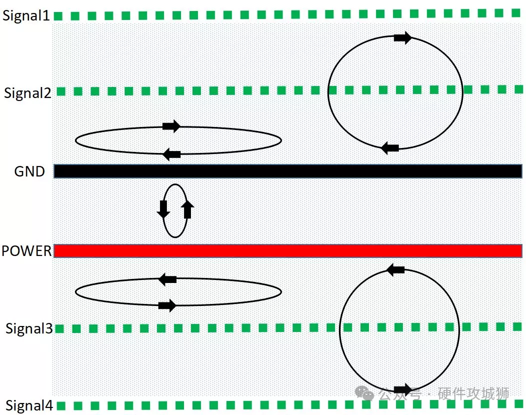
Alternative Option 4 (High‑Performance Local Signals)
Analysis:
- Better than Option 3 for a small number of high‑requirement signals.
- Provides an excellent routing layer S2.
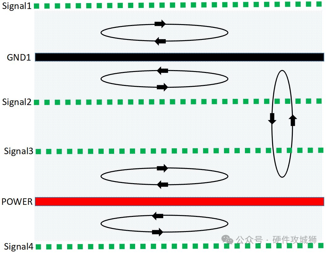
Option 2 (Worst EMC)
Analysis:
- S1 adjacent to S2; S3 adjacent to S4.
- None are adjacent to ground → very poor flux cancellation.
VI. Summary
PCB layer design rules for optimal EMC:
- Place a solid ground plane under the component side and solder side for shielding.
- Avoid two signal layers directly adjacent.
- All signal layers should be as close as possible to a ground plane.
- Critical signals (high‑frequency, high‑speed, clock) must have an adjacent ground plane.
About Maxipcb
Maxipcb empowers innovators to turn cutting-edge technologies into reality.
We offer one-stop solutions for design, simulation, testing, PCB manufacturing, component procurement and SMT assembly, enabling efficient development, rapid deployment and risk control across the full product lifecycle.Serving the world in communications, industrial automation, aerospace, automotive, semiconductor and beyond, we build a safer, more connected future together.