Well-designed interconnects are critical to realizing the full advantages of heterogeneous integration and chiplets.
Well-designed interconnects are critical to realizing the full advantages of heterogeneous integration and chiplets.
As the semiconductor industry shifts from monolithic planar chips to in-package chip and chiplet integration, interconnect design and manufacturing have grown far more complex—and increasingly vital to device reliability.
What was once a simple copper wire has evolved into tens of thousands of micro-bumps, hybrid bonding, through-silicon vias (TSVs), and even fiber-optic connections. The core goal remains unchanged: transmit signals from Point A to Point B as quickly as possible with minimal power and RC delay, while ensuring signals arrive intact. Making this work at scale is an ever‑growing challenge.
As data rates rise, we push the limits of what physical channels can carry, requiring parallel or nested parallelism to boost speed—and that means far more interconnects than ever before.
This is especially true for chiplets, where data must flow in and out to connect with other components in the package. While this approach is more complex, it delivers significant power benefits.
“Standard chips have high-power drivers on their output pins, strong enough to drive electrical signals across relatively large and long signal traces on a PCB,” said Marc Swinnen, director of product marketing at Ansys’ Semiconductor division. “But chiplets don’t need those large drivers, because 2.5D interconnects are much shorter. You can use smaller I/O drivers on each chiplet, saving both space and power.”
The main driver for this shift is the physics of packing more functionality into a fixed area. While digital logic scales down to single angstroms, shrinking wire dimensions increases resistance and capacitance, introducing new physical effects. Devices run hotter, signals slow down, and signal integrity becomes harder to maintain. Overcoming these issues requires new materials with higher electron mobility and wider critical data paths, plus deep insight into device behavior under varying workloads—all of which affects the full 3D layout of interconnects.
“You break down what was on a single die into multiple chiplets across a wider footprint,” said Frank Schirrmeister, vice president of solutions and business development at Arteris. “The on‑chip communication scheme must scale to inter‑chiplet communication, regardless of the substrate used. The complexity of on‑chip modules has already increased.”
As chips grew larger in the late 1990s, the industry focused on how to connect them, leading to virtual socket integration schemes and custom buses for every scenario. As block counts became unmanageable, test buses, high‑performance buses, peripheral buses, and more emerged. Over time, bus systems became too power‑hungry, spurring the development of protocols to reduce overhead.
Arm addressed this by creating the Advanced Microcontroller Bus Architecture (AMBA), an open standard for connecting and managing modules in SoCs. Over 30 years, AMBA has been revised and expanded with multiple secondary protocols. Most recently, Arm announced the new CHI C2C specification, extending AMBA to chiplets.
Interconnect Protocols
There’s irony in the wealth of interconnect PHYs and protocols available.
“One huge early advantage of monolithic chips was that there were no real interconnects,” Swinnen said. “Technically there were, but they were all built in one process step. A rule says system reliability degrades as the number of interconnects rises. Yet now we have far more connections—even a typical 2.5D design can easily have 500,000 bumps.”
Furthermore, reliability complications may be unavoidable, noted Andy Heinig, head of the Efficient Electronics department at Fraunhofer IIS’ Adaptive Systems Engineering.
“At some point, assembly technologies evolve—for example, from solder balls to copper pillars, then to hybrid bonding. With new assembly techniques, we may see new reliability issues. Chiplet interfaces pose new challenges here, as the number of interconnects in a given area is quite high.”
Yet well‑designed interconnects remain essential to unlocking heterogeneous integration and chiplet benefits. As more signals and larger data volumes must travel through increasingly complex layouts, interconnects can become bottlenecks due to added delay from so many connections.
“Your speed is determined by the slowest interconnect in your design,” noted Mick Posner, vice president of product management for High‑Performance Computing IP Solutions at Synopsys.
Interconnect Classification and Hierarchy
In multilayer integrated circuits, thin, short local interconnects provide on‑chip connections, while thick, long global interconnects carry signals between different blocks. As detailed by Larry Zhao, CTO at Lam Research, through-silicon vias (TSVs) enable signals and power to move vertically between layers.
The key difference between 2.5D (and future 3D‑IC) chiplet interconnects and traditional PCB interconnects is that 2.5D uses thinner, denser, and often shorter interconnects. New features like TSVs, micro‑bumps, and hybrid bonding further complicate the interconnect landscape—especially for 3D integration.
“On the plus side, communication between 2.5D chiplets is faster, higher‑bandwidth, and lower‑power than on a PCB,” Swinnen said. “The downside is that it’s more expensive than PCB technology. Many high‑speed signals require full electromagnetic coupling analysis, which is more complex than the simpler RC modeling you can use when signals stay on‑chip.”
Issues like IR drop and RC delay also degrade performance. To combat this, the industry is moving toward backside power delivery, reducing routing congestion on the device’s metal layers. This helps preserve signal integrity and ensure transistors receive sufficient power—but adds an entirely new layer of complexity not yet fully solved in high‑volume manufacturing.
As standards evolve and detailed variants emerge, choosing interconnect solutions has grown more complicated, even with defined nodes.
“When you look at interconnects within an SoC, you immediately think of things like the AMBA bus,” said Posner at Synopsys. “This has evolved with streaming interfaces, extensions like CHI, and expansion to more networks on the chip.”
Arteris focuses on scalability for heterogeneous, block‑to‑block topologies and mesh topologies that partition SoCs across multiple chips.
“It’s a process complicated by protocols—and further muddled by conflicting adoption of versions,” Schirrmeister said. “Most companies working with RISC‑V have adopted CHI, so the question is in the details: which version are they using? For example, the latest Arm cores have CHI‑e interfaces, while older Arm cores have CHI‑b. You run into versioning, with different features in different releases.”
This makes communication and compatibility critical.
Streamlining Interconnect Protocol Options
The proliferation of protocols is unlikely—and should not—to be curbed anytime soon, said Debendra Das Sharma, Intel Senior Fellow and Co‑General Manager of Memory and I/O Technology.
“Some mistakenly believe there should be one interconnect to rule them all. That is incorrect. I believe the industry has rallied around the right set of interconnects: UCIe for intra‑package, PCIe and CXL for off‑package, rack/pod‑level, and Ethernet for networking.”
It is therefore critical that all these interconnects can communicate with one another, and interoperability remains an essential goal for designers.
“To address these challenges with multiple interconnects, the industry truly needs interoperable standards that scale vertically and horizontally,” said Priyank Shukla, lead product manager for Interface IP at Synopsys. “The entire ecosystem is working to align and match this performance. We see the Ultra Ethernet Consortium providing a backend network that scales horizontally, while AMD offers open fabrics and CXL technologies enabling cache coherence. For die‑to‑die partitioning, UCIe is the best choice. These interoperable open standards provide innovation to address the interoperability challenges facing the industry.”
Chiplets
While implementations vary, there is a clear trend toward standardization for chiplet interconnects.
“Even users with connections on both ends tend to adopt standards, because they want to benefit from the collective work done by large standards bodies such as UCIe,” said Mayank Bhatnagar, director of product marketing at Cadence Silicon Solutions Group. “We will never have enough engineers to design every possible interconnect, and relying on standards allows users to learn from the collective work of others in the field.”
At the same time, tight supply chains for advanced packaging have pushed more users to consider organic packaging.
“Organic packaging, also known as standard packaging, enables shorter turnaround times, and the supported bandwidth density can meet the needs of many customers who initially thought their designs required advanced packaging,” Bhatnagar said.
Still, a critical unresolved issue remains as the industry moves toward chiplets.
“A very important challenge for chiplet interconnects comes from the fact that no one can test the interface by probing with needles or a probe card as before,” noted Heinig at Fraunhofer. “Such testing is necessary if bring‑up fails or errors occur during operation. Here we need new solutions, such as on‑chip monitoring and test.”
Addressing New Complexities
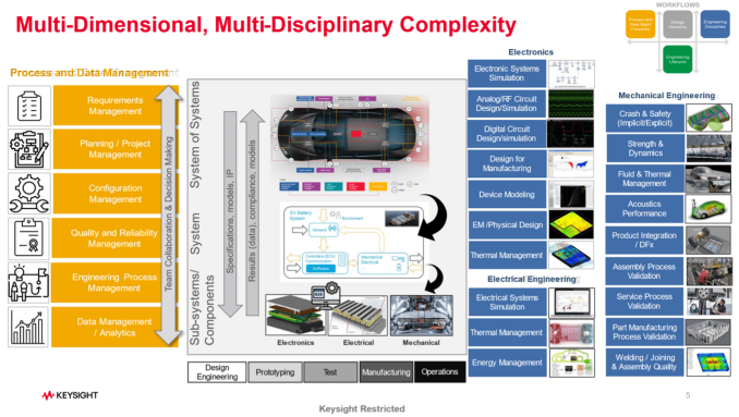
As new 2.5D/3D package designs grow more complex, demand for new solutions is intense. Product development has become cross‑disciplinary, bringing together diverse specialties and analysis tools.
“High‑speed digital, RF, photonics, power electronics, ASIC design, thermal, mechanical, and more must all be tightly integrated,” said Mueth at Keysight Technologies. “This is one dimension of complexity; these disciplines are often interdependent, further complicating the design process. Requirements, processes, and data must be managed across the entire engineering lifecycle of design, test, and manufacturing, adding more complexity to product development. Finally, chiplets must operate within a higher‑level hierarchical system, so top‑down design and bottom‑up verification elements must be considered.”
About Maxipcb
Maxipcb empowers innovators to turn cutting-edge technologies into reality.
We offer one-stop solutions for design, simulation, testing, PCB manufacturing, component procurement and SMT assembly, enabling efficient development, rapid deployment and risk control across the full product lifecycle.
Serving the world in communications, industrial automation, aerospace, automotive, semiconductor and beyond, we build a safer, more connected future together.


