With the rapid development of electronic technology, the miniaturisation and micro‑miniaturisation of electronic components, as well as the increasing prevalence of high‑density chips with pitches of 0.3 mm to 0.5 mm, have imposed ever‑higher requirements on electronic soldering techniques.
With the rapid development of electronic technology, the miniaturisation and micro‑miniaturisation of electronic components, as well as the increasing prevalence of high‑density chips with pitches of 0.3 mm to 0.5 mm, have imposed ever‑higher requirements on electronic soldering techniques. Although more precise pick‑and‑place machines can now replace manual soldering, there are still many factors that affect soldering quality. From the perspective of SMT assembly, this article introduces several key points that should be noted during PCB design. Based on experience, failure to follow these recommendations may result in poor soldering quality, cold solder joints, and even damage to pads or the circuit board during rework.
I. Factors Affecting PCB Soldering Quality
From PCB design to the completion of a high‑quality assembled board, strict control is required across many stages, including PCB design, soldering process, and operator skill. The main factors include: the PCB layout, the quality of the bare board, component quality, oxidation level of component leads, solder paste quality, solder paste printing quality, accuracy of pick‑and‑place programming, placement quality of the machine, reflow oven temperature profile, and more. One critical stage that the assembly house cannot bypass is the PCB design phase. Since circuit designers often do not solder boards themselves, they lack direct practical soldering experience and may not be aware of the various factors affecting soldering quality. Conversely, assembly operators do not understand PCB layout; they simply complete production tasks and have neither the inclination nor the ability to analyse the causes of poor soldering. As these two groups work in separate domains, it is difficult to integrate their knowledge effectively.
II. Recommendations for PCB Layout
Below are some suggestions for PCB layout engineers, with the aim of avoiding design practices that compromise soldering quality. These are presented mainly with illustrated examples.
1. Tooling Holes: Four holes (minimum diameter 2.5 mm) should be placed at the four corners of the PCB for positioning during solder paste printing. The centres of the holes on each axis (X or Y) should be aligned. See figure below:
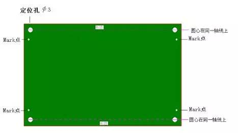
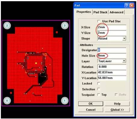
2. Fiducial Marks (Mark Points): Fiducial marks are required for pick‑and‑place machine alignment. Place Mark points at diagonal corners of the board – they can be round or square pads, but must not be confused with component pads. If components are on both sides, Mark points should be provided on both sides. When designing the PCB, note the following:
a. Mark points should have a shape such as those shown (symmetric top‑bottom or left‑right).
b. Dimension A should be 2.0 mm.
c. Within 2.0 mm from the outer edge of the Mark point, there should be no shapes or colour changes that could cause erroneous recognition (pads, solder paste).
d. The Mark point should have good contrast with the surrounding PCB colour.
e. To ensure recognition accuracy, the Mark point surface should be plated with copper or tin to prevent reflection. Marks consisting only of lines cannot be recognised by the optical system. See figure below:
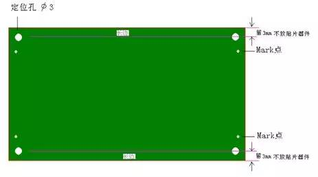
3. 5 mm Edge Clearance: When drawing the PCB, leave a minimum 3 mm clearance along the long edge for the conveyor rails of the placement machine. No SMD components should be placed in this area, as the machine cannot place there. See figure:
For double‑sided boards, consider that during the second reflow pass, components near the edge on the already soldered side may be knocked off, and in severe cases, pads or the board itself may be damaged. See figure:
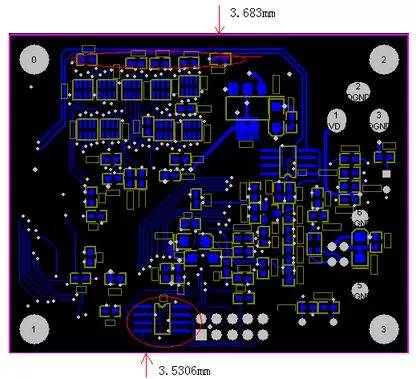
Therefore, it is recommended that on the side with fewer chips (usually the Bottom side), no SMD components be placed within 5 mm of the long edge. If board space is limited, consider adding a break‑away rail (see item 17 on panelisation and rails).
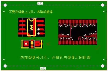
4. Do Not Place Vias Directly in Pads: The drawback of placing vias directly in pads is that during reflow, molten solder can flow into the via, leaving insufficient solder on the pad and causing a cold solder joint. See figure:
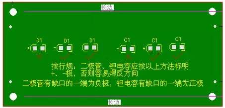
5. Polarity Marking for Diodes and Tantalum Capacitors: Polarity markings for diodes and tantalum capacitors should follow industry standards to prevent assembly operators from soldering them in the wrong orientation based on habit. See figure:
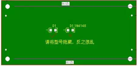
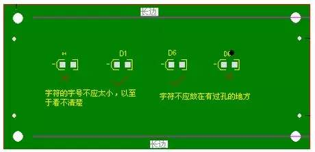
6. Silkscreen and Identifiers: Hide component type numbers (e.g., "104", "0805") on the silkscreen, especially on high‑density boards, to avoid visual clutter that makes it difficult to locate placement positions. See figure:
Also, do not label only the type number without the reference designator (e.g., "R1", "C2"), as this prevents correct programming for the placement machine. See figure:
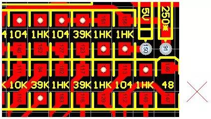
The font size of silkscreen text should not be too small to be legible. Position text so that it does not overlap vias, which could cause misreading.
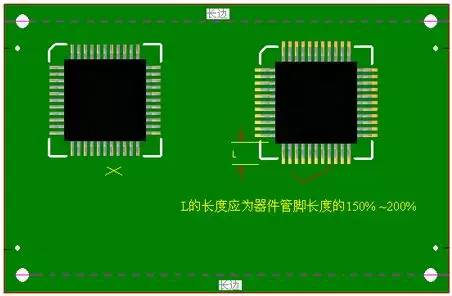
7. Extend IC Pads (Length): For SOP, PLCC, QFP, and similar packages, the PCB pad length should be extended. A suitable length is approximately 1.5× the length of the IC lead. This facilitates manual soldering with an iron, allowing the lead, pad, and solder to fuse properly. See figure:
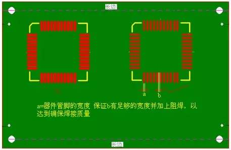
8. IC Pad Width: For SOP, PLCC, QFP, and similar packages, pay attention to pad width. The PCB pad width (a) should equal the nominal lead width given in the datasheet. Do not increase it, so as to maintain sufficient clearance (b) between pads and reduce the risk of solder bridging. See figure:
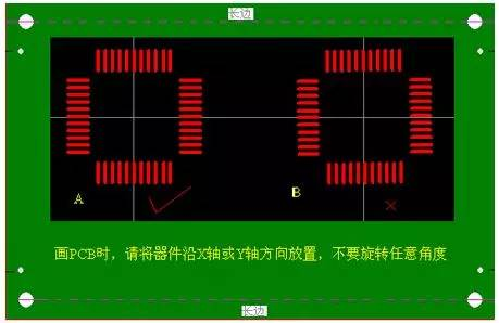
9. Avoid Arbitrary Component Rotation: Placement machines can only rotate components by 90°, 180°, 270°, or 360° – they cannot handle arbitrary angles. For example, if a component is rotated by 1° as shown in Figure B, the leads will be misaligned with the pads by 1°, affecting soldering quality. See figure:
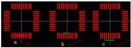
10. Shorting Adjacent Pins: The method shown in Figure (a) is not ideal, as it does not clearly indicate which pins should be shorted, and the result is not aesthetically pleasing. If the shorting is done as shown in Figure (b) or (c), with solder mask applied, the result is much better: as long as each pin is not bridged, the chip will have no shorts and the appearance is neat. See figure:
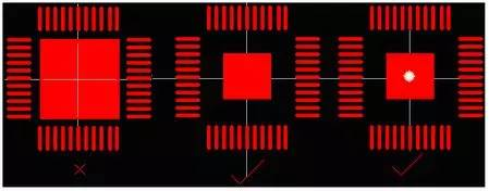
11. Center Pad Under the Chip: For ICs with a centre pad underneath, if you follow the exact footprint, it may increase the risk of shorts. It is advisable to reduce the size of the centre pad slightly, increasing the clearance to the surrounding peripheral pads and thus reducing short‑circuit opportunities. See figure:
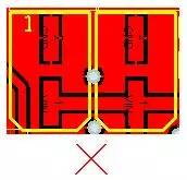
12. Avoid Placing Tall Components Close Together: As shown in the figure, placing two tall components too close together may cause the placement machine head to collide with the first component when placing the second, triggering a safety alarm and shutting down the machine. See figure:
13. BGA Considerations: Since BGA pads are hidden under the chip, soldering quality is not visible. For ease of rework, it is recommended to place two positioning holes (Hole Size: 30 mil) on the PCB to align the stencil used for solder paste printing during rework. The hole size should be appropriate – the pin should not fall out or wobble when inserted; a snug fit is ideal for accurate alignment. See figure:
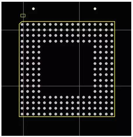
It is also advisable to leave a clear area around the BGA, free of other components, to accommodate the stencil during rework.
14. PCB Colour: Avoid using red solder mask, because under the red light of the placement machine's camera, a red board appears white, making programming difficult and hindering machine operation.
15. Small Components Under Large Components: Some designers place small components (e.g., resistors) under large components on the same side – for example, resistors under a 7‑segment display. This makes rework very difficult, as the large component must be removed first, risking damage. It is better to place such small components on the Bottom side, as shown. See figures:
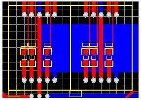
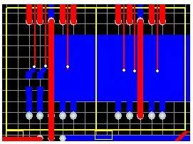
16. Copper Pour Near Pads Affecting Solder Melting: Large copper areas absorb significant heat, preventing solder from melting fully and causing cold solder joints. In Figure (a), the pad is directly connected to a large copper pour. In Figure (b), although the 50‑pin connector pad is not directly connected to copper, the inner layers of the 4‑layer board are large copper planes, so both cases suffer from excessive heat sinking. The connector body in Figure (b) is made of plastic that cannot withstand high temperatures; if the reflow temperature is set too high, the connector may melt or deform, while if set too low, the copper absorbs too much heat and the solder does not melt properly. Therefore, it is recommended to isolate pads from large copper areas, as shown. See figures:
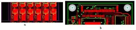
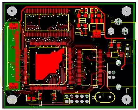
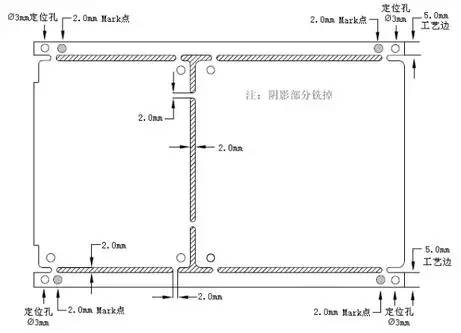
17. Panelisation and Break‑Away Rails:
III. Summary
Nowadays, more and more engineers are capable of using CAD software to draw, route, and design PCBs. However, to ensure that the design not only is completed but also facilitates high‑efficiency soldering, the author believes that the points above must be given due attention. Cultivating good layout habits and maintaining effective communication with the manufacturing facility are considerations that every engineer should bear in mind.
About Maxipcb
Maxipcb empowers innovators to turn cutting-edge technologies into reality.We offer one-stop solutions for design, simulation, testing, PCB manufacturing, component procurement and SMT assembly, enabling efficient development, rapid deployment and risk control across the full product lifecycle.
Serving the world in communications, industrial automation, aerospace, automotive, semiconductor and beyond, we build a safer, more connected future together.
