This article discusses two pad design schemes for multi-layer PCBs: the half-covered & half-exposed design and the equal-size design.
This article discusses two pad design schemes for multi-layer PCBs: the half-covered & half-exposed design and the equal-size design.
Half-covered & Half-exposed Design
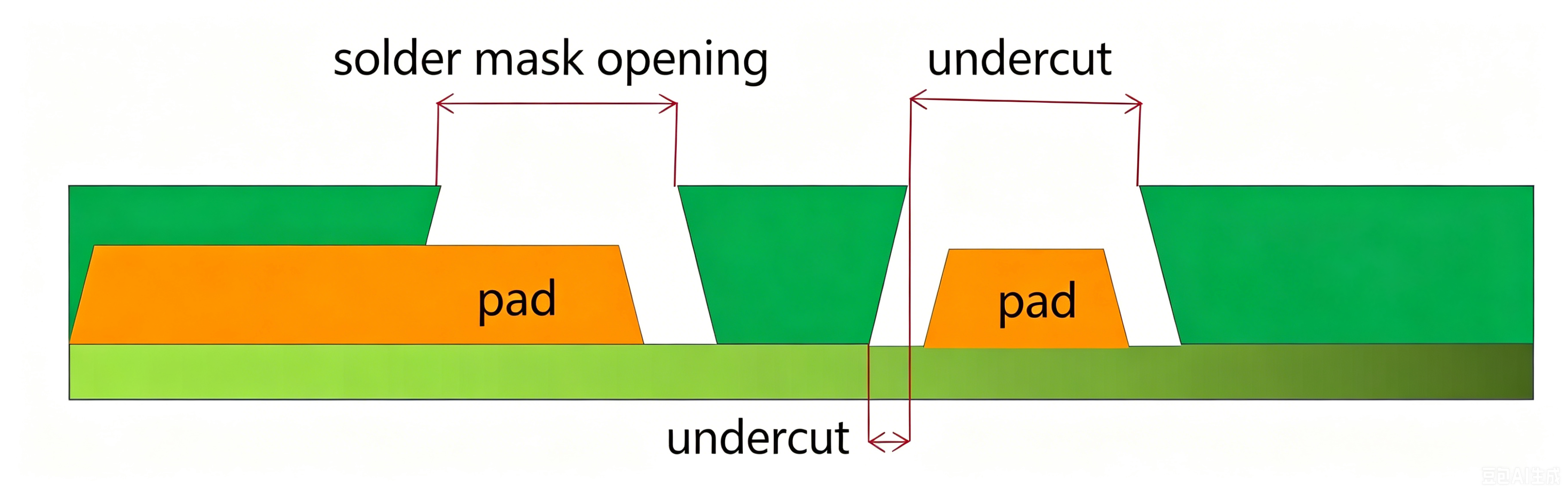
As the name suggests, part of the pad is covered by solder mask ink, while the other part is exposed.
For details, refer to the figures below:
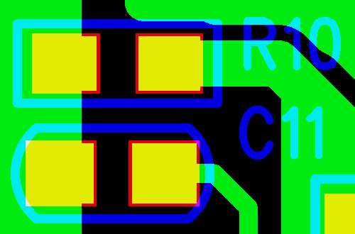
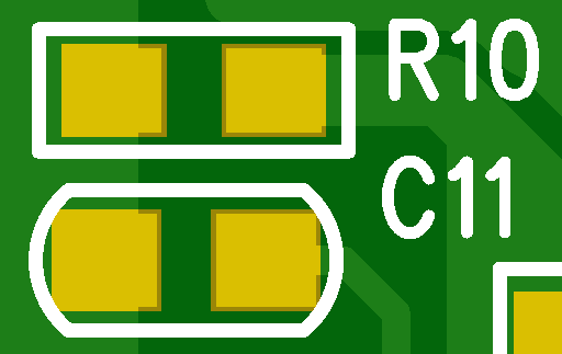
Simulation Diagram
Cross-section Diagram
Solder mask opening, solder mask opening; pad, pad; side etching
This design is generally not used under normal conditions. However, if the pad and solder mask opening are relatively large, the impact is negligible and the design is acceptable. In contrast, if the pad and solder mask opening are small, the impact will be significant, and the most common problem is
pad deformation (see the figure below).
(Note: Round pads become irregular, with inconsistent sizes and shapes.)
Nevertheless, this design is difficult to avoid completely. PCB manufacturers can only adopt local differential compensation for optimization, but cannot guarantee a full resolution. Therefore, in such cases, the design shall be validated against the actual performance of the PCB in PCBA mass production.
Equal-size Design
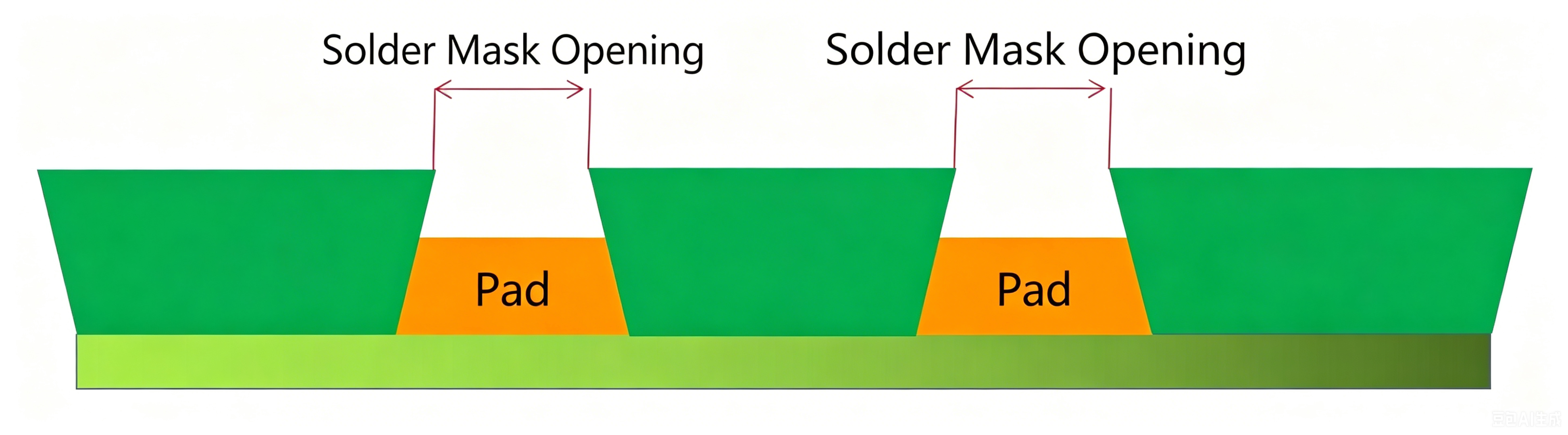
Equal-size design means the pad size is identical to the solder mask opening size.
However, experienced designers generally consider this an incorrect design practice.
Cross-section Diagram
Solder mask opening, solder mask opening; pad, pad
(Note: No design or simulation diagrams are available, as no equal-size pad design documents have been submitted by readers.)
Why?
From a design perspective, this does not seem problematic, but in actual manufacturing, the equal-size design is nearly unproducible, which leads to quality issues. Therefore, experienced designers usually avoid this scheme.
So why is this design almost unmanufacturable?
This is related to the process tolerances of pad-related processes in PCB manufacturing.
During PCB layout, designers often fail to account for all process tolerances in actual production due to limited knowledge. However, these tolerances are real in PCB manufacturing and will affect the final product quality.
If a PCB pad is designed with the equal-size scheme, most manufactured pads will end up in the following state: solder mask ink will inevitably cover one side of the pad, reducing the actual usable area of the pad and causing troubles in subsequent PCBA production, such as cold solder joints.
To summarize: pads should preferably be designed as
full-covered pads or
full-exposed pads if conditions allow. If not feasible, the half-covered & half-exposed design can be adopted, and the PCB manufacturer shall be notified to perform local compensation and optimization. The equal-size design should be avoided as much as possible.
About Maxipcb
Maxipcb empowers innovators to turn cutting-edge technologies into reality.
We offer one-stop solutions for design, simulation, testing, PCB manufacturing, component procurement and SMT assembly, enabling efficient development, rapid deployment and risk control across the full product lifecycle.Serving the world in communications, industrial automation, aerospace, automotive, semiconductor and beyond, we build a safer, more connected future together.