
If the Package Is Wrong, No Matter How Beautiful the Routing, It Won’t Fit
You find a package online with the same pin count and a similar name—can you just drop it into the PCB? Don’t rush. A package is not just an outline on the screen; it also defines pad positions, numbering, and how the device lands on the board. The same pin count does not necessarily mean it will fit; a similar shape does not necessarily mean it is connected correctly. For those just starting to draw boards, the most useful thing is not memorizing a long list of package abbreviations, but establishing two independent check lines: electrically, whether every functional pin is connected to the correct pad; mechanically, whether the physical part you bought can be assembled as expected. Only when both pass do you have a reliable starting point for routing.
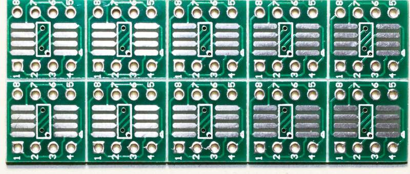
Figure 1: An SOIC-to-DIP adapter board uses different pad arrangements to connect different packages.
First Confirm Which Complete Part Number You Bought
When you get a chip name, first ask: is this just a device family, or is it a complete orderable part number? The same family may have different packages, temperature grades, and packing forms. Suffixes often contain important information, but naming methods differ between manufacturers and cannot be guessed from experience. In the original manufacturer’s datasheet or ordering information, map the complete part number to a clear package name and package drawing.
Then look at the library file. A package called “8-pin chip” at least does not tell you whether it is through-hole or SMD, how far apart the two rows of pins are, or what the pin pitch is. Even if the name says DIP or SOIC, you still need to look at the specific dimensional version. The adapter board in Figure 1 illustrates exactly this: the circuit can use traces to connect two arrangements, but the two packages are not the same physical object.
It is worth keeping a record here: complete part number, manufacturer, datasheet version, and the library name used. Later, when purchasing alternative devices or when someone else takes over the design, they will know why this package was usable in the first place, rather than being left with only “downloaded from the internet.”
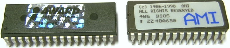
Figure 2: Physical appearance of a dual in-line package; even with two rows of pins, you cannot select a package based only on pin count.
Connect Functional Pins, Symbol Numbers, and Pad Numbers
The schematic symbol expresses circuit relationships, and the PCB package describes the pads on the board. Software usually establishes the correspondence through pin numbers and pad numbers. You cannot assume the mapping is correct just because the symbol looks good. Functions such as power, ground, input, and output must be traceable from the datasheet all the way to the symbol, and then to the PCB pad.
Figure 3 gives a top-view pin example of a 741 8-pin package. At this point, you need to look at the notch or orientation mark, the numeric numbering, and the function names together. A top view is viewed from above the device; if you mistakenly treat a bottom view as a top view, the left-right relationship may be reversed. Do not just remember “pin 1 is at the upper left”; first confirm which side this drawing is viewed from.
A useful checking method is to write each pin as a row: function and number in the datasheet, number in the symbol, and pad number in the package. After corresponding row by row, check whether unconnected pins and special pads have clear explanations. Software checks can find some connection errors, but they cannot prove for you that the numbering in the library was drawn correctly in the first place.
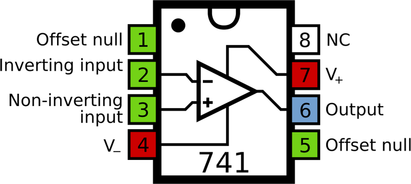
Figure 3: Top-view pin example of a 741 8-pin package; the notch, numbering, and functions need to be checked together.
Check Dimensions, and Leave Space as Well
After the electrical relationships are correct, check the mechanical assembly. Prefer comparing with the manufacturer’s package dimension drawing: check pin pitch, the span of two or more rows of pins, body outline, and the shape of the solder terminals. Units are especially easy to overlook: millimeters and inches cannot be mixed, and the minimum and maximum values in dimension callouts cannot be casually treated as the same number.
The four-side pin device in Figure 4 visually looks like just a ring of dense pins. What really determines whether it can be assembled, however, is the specific pitch, outline, and pad arrangement. The package dimension drawing describes the device itself, while the recommended land pattern drawing describes how the board receives the device; the two have different purposes. When a recommended land pattern is available, verify it against the specific process rather than treating the outline of the device’s metal leads as the pad itself.
Also move your view around the device. Is there space for connector insertion and removal? Will tall components press against the enclosure? Can subsequent soldering and rework access the area? These may not all be found by ordinary electrical rule checks. For the first board, confirming special devices with the assembly side early is more effective than waiting until the board comes back and then figuring something out.
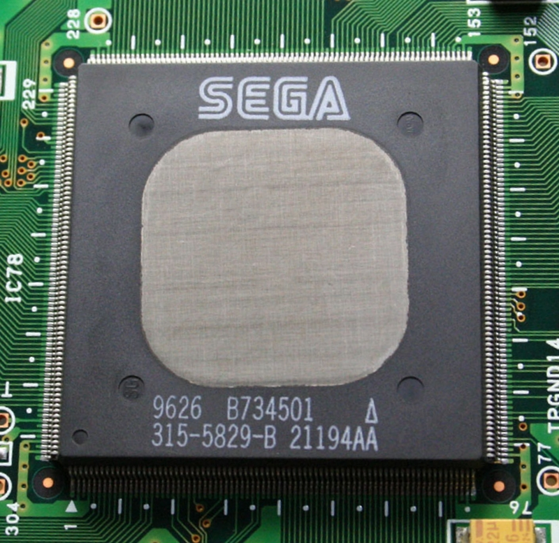
Figure 4: Physical four-side pin package; dense pins require item-by-item verification of pitch and outline.
Do a Small Verification Before Starting Large-Area Routing
Package checking does not require building a complex process from the start. You can first pick the devices most likely to go wrong in this project, such as newly created library chips, connectors, or materials intended as substitutes, and check them by “identity—numbering—orientation—dimensions.” Do not use the fact that other devices passed verification to infer that all packages on the board are reliable.
If you already have the physical part, you can print the board footprint at true scale, first confirm that the printing software has not automatically scaled it, and then verify the scale using a known dimension. Place the physical part on it and compare the outline and pin positions; this can help find obvious errors. However, paper comparison cannot prove soldering quality, nor can it replace checks of dimensional tolerances, recommended land patterns, and manufacturing requirements.
Finally, fix the problems you find back into the library and records, rather than only temporarily moving a few pads in the current PCB. Otherwise, the next project may still call the old error. Figure 5 puts the two check lines together: electrical mapping answers “is it connected correctly?”, and mechanical assembly answers “will it fit and assemble well?” These are two questions, and one cannot replace the other.
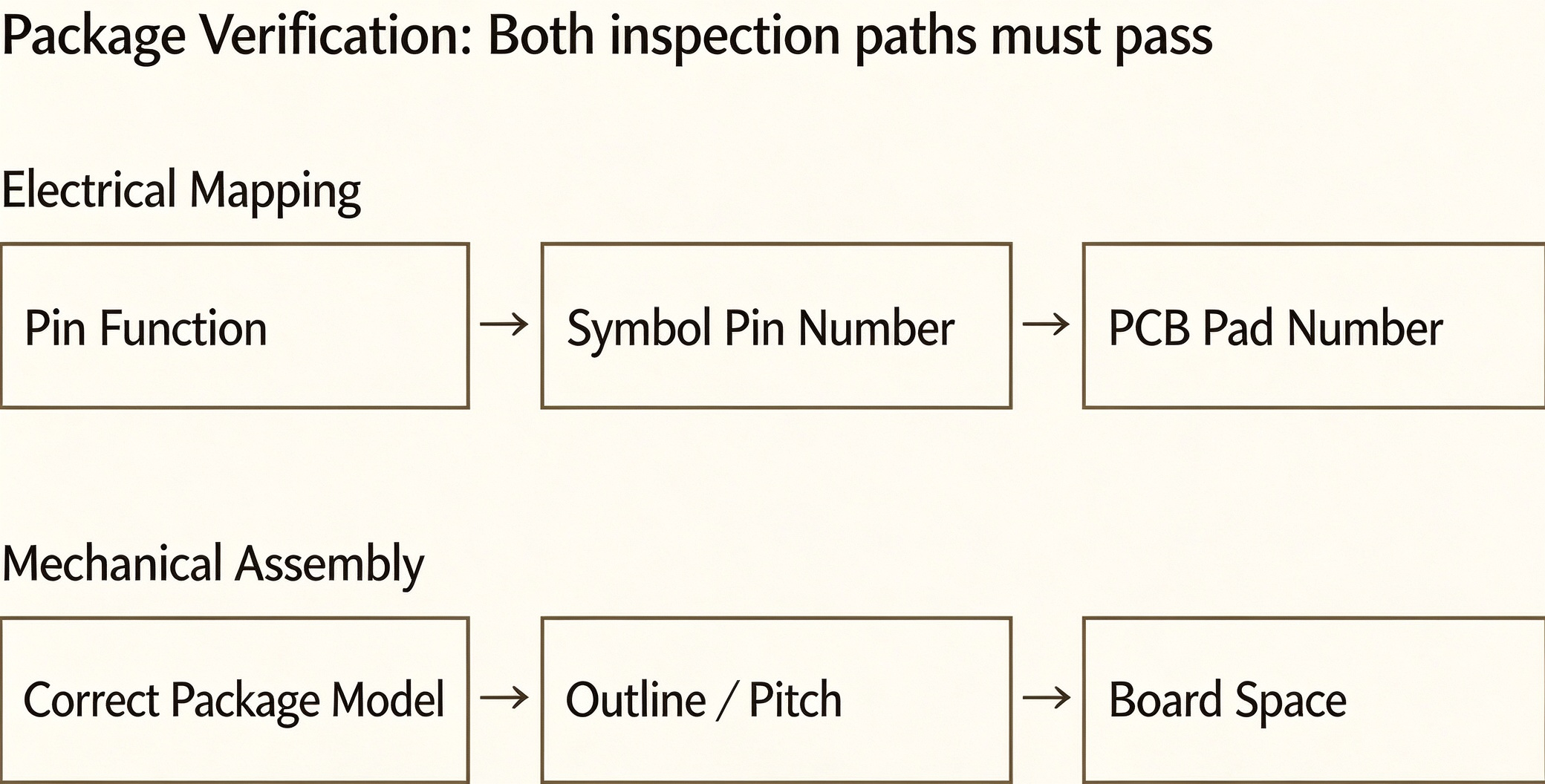
Figure 5: Package verification must connect both check lines: electrical mapping and mechanical dimensions.
The end point of package verification is not “the software reported no errors,” but that the complete part number, pin mapping, and assembly dimensions are documented and verifiable. The next time you are about to start routing, spend ten-plus minutes checking a newly used device and keep the verification results in the project record. If you find uncertain items, clarify them before continuing. On the board in your hands, which device’s package was selected only by name and has not yet been checked against the complete part number and dimension drawing?