The schematic is done and the components have been imported into the PCB. Facing a tangled mess of ratlines, do you not know which one to move first? Some people put the large chip in the middle first, some arrange components around the board edge, and others stuff them wherever there is space.
The schematic is done and the components have been imported into the PCB. Facing a tangled mess of ratlines, do you not know which one to move first? Some people put the large chip in the middle first, some arrange components around the board edge, and others stuff them wherever there is space. The truly useful starting point is to first distinguish which positions cannot be moved, which components must be next to each other, and which areas must be reserved. Layout is not about arranging components neatly; it is about planning in advance how the circuit will connect, how the board will be assembled, and how it can be accessed during debugging. For a first low-voltage small board, you can do one round of layout according to the following four types of positions, and then start large-area routing.
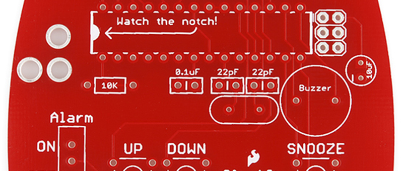
Figure 1: Local view of a bare board for a clock circuit; the positions of buttons and the buzzer affect the arrangement of surrounding devices.
Type 1: First Lock Down Positions That “Cannot Be Moved Casually”
First look at the board outline and mechanical requirements, then look at component sizes. Mounting holes, buttons aligned with the enclosure, display windows, and external connectors usually determine their positions earlier than the main control chip. Interface plugs also need insertion and removal space; you cannot only check whether the pads fit on the PCB. When dimensions are not confirmed, mark them as pending confirmation first; do not treat guesses as fixed conditions.
At this step, you can write three sentences next to the board outline: where the board is installed, from which side the user operates it, and from which side cables enter and exit. Even for a practice board, these boundaries should be artificially defined. Otherwise, the layout may look compact, but later half the board may need to be moved again for the orientation of one plug. If you have the actual connector on hand, compare it with the package dimensions and insertion direction; if you only have an online shop photo, do not estimate by visual proportions. Dimensional information must be confirmed against the device mechanical drawing and mechanical documentation.
Figure 2 shows the devices just imported in the tutorial. The components being present does not mean layout has begun; the real first step is to bring in mechanical positions and functional requirements. The outline of a practice board can be iterated, but when a product already has an enclosure, the board outline cannot be changed casually to follow the components.
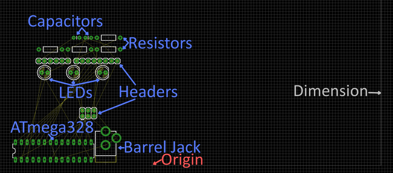
Figure 2: State when devices have just been imported into the board outline; ratlines indicate electrical connections still to be completed.
Type 2: Line Up Functional Blocks According to Connection Relationships
Divide the schematic into several parts whose purposes can be stated, such as power input, main control, sensor interface, display or indicator lights. First ask “who passes the signal to whom,” and then decide how close they should be to each other. What you arrange this way is not several isolated chips, but connection paths with starting points and endpoints.
The main control does not necessarily have to be placed at the geometric center. If most interfaces are concentrated on one side, placing the main control slightly closer to that side may make routing easier; if there are sensitive analog inputs, also consider keeping them at an appropriate relationship with noisy circuits. What is “appropriate” here depends on the actual circuit; it is not a universal rule of how many millimeters to separate them.
Ratline crossings can indicate whether placement is awkward, but they cannot determine good or bad by themselves. First identify critical connections, then try rotating or moving the entire functional block. Do not break already confirmed interface positions or local device requirements just to make all ratlines as short as possible.
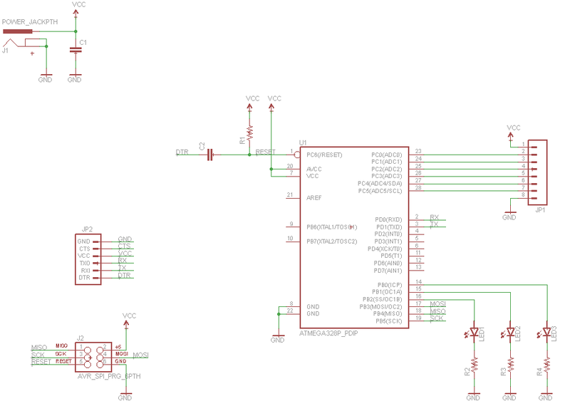
Figure 3: Schematic of the example board; use it first to identify functional blocks such as the main control, interfaces, and LEDs.
Type 3: Small Components Also Have Their Own “Fixed Partners”
Decoupling capacitors, clock-related devices, feedback resistors, etc. are often not small parts used to fill gaps at the end. Decoupling capacitors provide local support for fast current changes near the chip; if they are far from the power pin, the connection path may weaken the effect. Check the chip datasheet’s recommended layout first, then decide placement.
The layout in Figure 4 arranges the main control, connectors, LEDs, and resistors according to functional relationships. When reading the figure, focus on “which component serves which device”; there is no need to copy its absolute coordinates. The example uses relatively simple through-hole devices and cannot be directly treated as a standard layout for high-speed or high-density products.
A practical action is: circle these local small combinations on the schematic and try to move them together as a group during layout. After the main chip position changes, go back and check them again, rather than only moving the main chip away and leaving the peripheral devices in place.
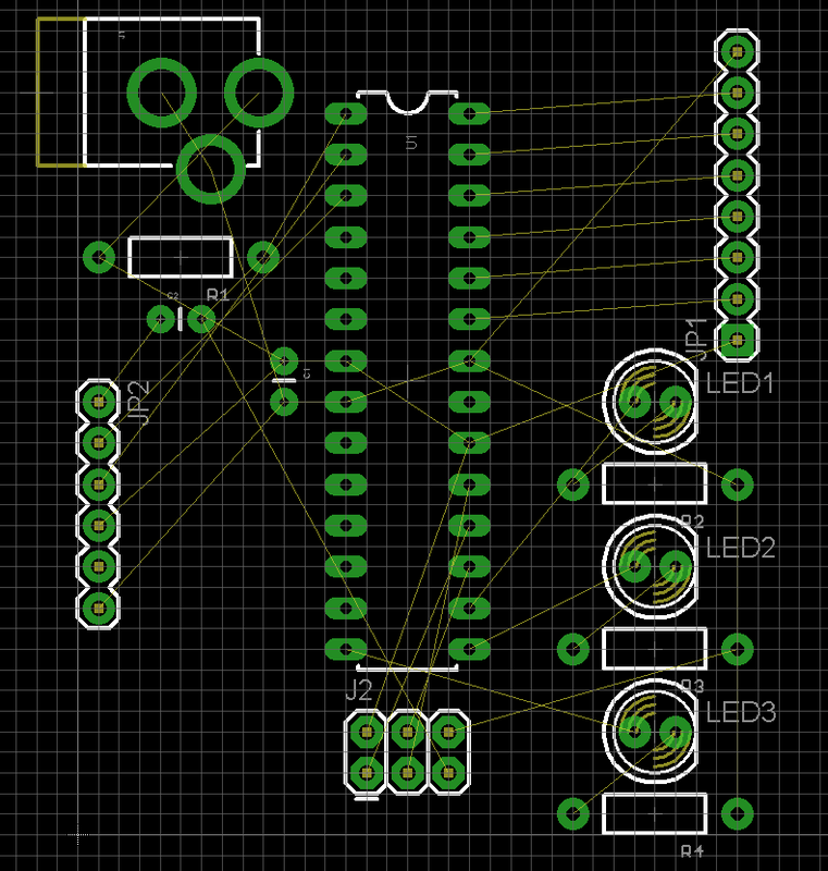
Figure 4: Component positions after placement according to functional relationships; the main control periphery is no longer arbitrary gap-filling.
Type 4: Leave Entrances for Routing, Soldering, and Debugging
If you discover only after the components are fully placed that traces cannot get out, you usually have to go back and redo the layout. Before starting routing, look along several critical connections: are there channels blocked by components, can signals be led out smoothly near interfaces, and is there reasonable space for power and ground connections? Blank space is not necessarily waste; it may be a condition for completing the design later.
Also simulate actual use: can the download cable be connected, can common test points be touched, and are polarity markings clear? For areas requiring manual soldering or rework, reserve operating space according to the device package and assembly method; for mass production requirements, confirm with placement, test, and mechanical personnel; a single universal spacing rule cannot cover everything.
Figure 5 shows the same tutorial design after routing is completed. It reminds us that the value of layout must ultimately be tested by whether connections can be completed smoothly. Basic rule checks still need to be done, but this round is not about solving all process problems first; it is about giving the placement order a basis and giving rework a direction.
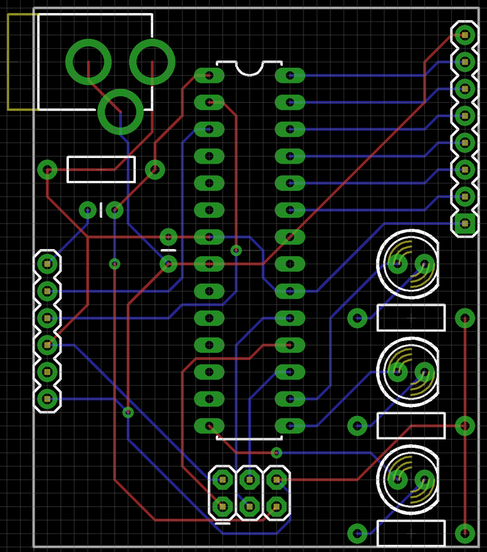
Figure 5: Board diagram of the same example after routing; review which placement arrangements helped the connections.
In layout, arrange constraints first, then pursue compactness. The next time you open a PCB, you might first use four types of marks to distinguish fixed positions, functional blocks, local partners, and reserved areas, clarify the most uncertain dimensions first, and then proceed to routing. This sequence is an introductory checking method and does not replace the design requirements of specific chips and products. On the board in your hands, what determines the layout first: external interfaces, mechanical mounting, or a certain critical connection?
About Maxipcb
Maxipcb empowers innovators to turn cutting-edge technologies into reality.We offer one-stop solutions for design, simulation, testing, PCB manufacturing, component procurement and SMT assembly, enabling efficient development, rapid deployment and risk control across the full product lifecycle.
Serving the world in communications, industrial automation, aerospace, automotive, semiconductor and beyond, we build a safer, more connected future together.
