
Long-term failures of HDI PCBs are usually not caused by a single defect, but by the combined effects of materials, lamination processes, copper distribution, dielectric layer thickness, moisture, contaminants, and operating stress.
During the design stage, manufacturing risks, mechanical risks, and potential electrochemical failure mechanisms must be evaluated simultaneously.
When engineers discuss the reliability of high-density interconnect (HDI) designs, microvia cracks are often the focus. Thermal cycling stress, coefficient of thermal expansion mismatch, and copper fatigue are all well-documented failure modes. With material improvements, process control, and optimized design rules, these failures have been managed more and more effectively.
Microvia cracks are not the only way HDI designs fail in real applications. HDI failures can arise from more subtle mechanisms: mechanisms that may not appear in standard qualification tests but are exposed only after months or years of product use. Understanding these deeper causes helps designers anticipate and prevent failures that traditional reliability analysis may miss.
Resin Starvation
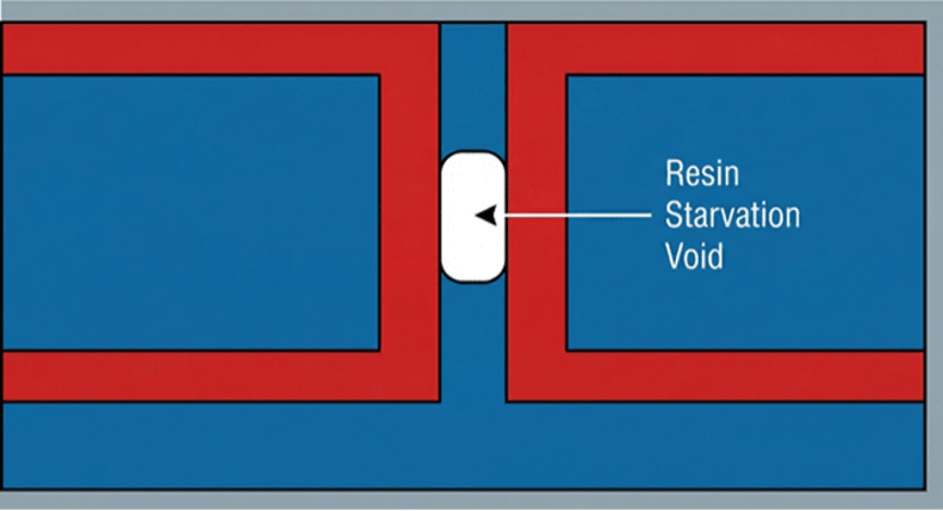
Figure 1: Resin starvation
During lamination, the resin in the prepreg layers flows to fill gaps, encapsulate copper features, and bond the layers together. When the available resin is insufficient to fill all voids, resin starvation occurs, creating defects such as unfilled cavities, incomplete interlayer bonding, or insufficient encapsulation of buried structures.
Resin starvation is especially common in HDI designs for several reasons. Sequential lamination cycles gradually consume the available resin: resin in the prepreg has already flowed in the previous lamination cycle, and less resin remains available to flow in subsequent cycles. Compared with designs with sparse copper distribution, high-density copper features—especially filled via pads and large-area thick copper regions—occupy more space and require more resin to complete filling. The narrow gaps formed by fine-pitch structures also make it harder for high-viscosity resin to penetrate fully.
The consequences of resin starvation range from minor to catastrophic. Mild resin starvation may cause local delamination that slowly propagates under thermal stress; severe resin starvation may leave voids that absorb moisture, creating conditions for conductive anodic filament growth or electrochemical migration between adjacent conductors.
Preventing resin starvation requires balancing copper density, selecting appropriate prepreg (resin content should match the copper occupancy volume), and optimizing the lamination process. Design for Manufacturing (DFM) tools can flag areas at risk of resin deficiency before manufacturing, enabling design modifications to improve resin flow.
Copper Foil Delamination Caused by Lamination Cycles
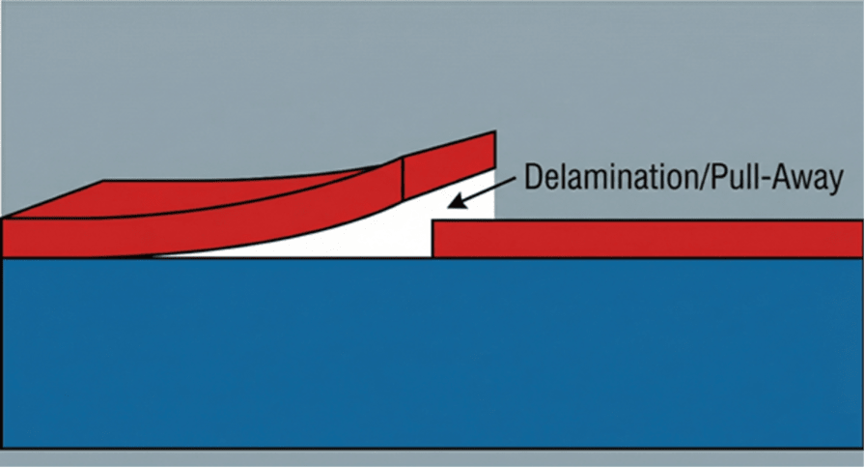
Figure 2: Copper foil delamination (separation)
Each sequential lamination cycle subjects existing copper features to another thermal stress shock. Copper and dielectric expand and contract at different rates; the adhesion at the copper-dielectric interface must withstand the resulting shear stress.
In a conventional single-lamination design, each interface experiences one lamination cycle and subsequent thermal events (reflow soldering, operating temperature cycling). In a 3-N-3 HDI design, the innermost core interface has already experienced four lamination cycles before the board even enters the assembly stage. Cumulative stress weakens the adhesion between copper and dielectric, especially at feature edges where stress concentrates.
Copper foil delamination typically appears as lifted pads, delaminated traces, or annular separation around vias. These defects may not cause immediate failure, but they create stress concentration that accelerates crack initiation under operating thermal cycling.
Material selection affects the likelihood of copper foil delamination. Different laminate systems differ in their ability to maintain interfacial bonding after multiple thermal cycles. Copper surface treatment (oxide, silane, or other adhesion promoters) also affects bond durability. For high-layer-count HDI designs, confirm that the selected material system has been validated for the required number of lamination cycles and can meet the sequential lamination count required by the stack-up.
Dielectric Crush Under High Mechanical Stress
HDI stack-ups often include very thin dielectric layers (only 2 to 4 mil thick) to achieve target impedance with narrow trace widths and to minimize overall board thickness. Under stress, these thin dielectric layers are more prone to mechanical deformation than thicker conventional layers.
When local pressure thins the dielectric layer beyond acceptable limits, dielectric crush occurs, which can cause copper features on adjacent layers to move closer together or even short-circuit. Sources of local pressure include:
Component mounting: press-fit connectors, heatsinks mounted with fasteners, and stiffening ribs all apply mechanical force to the board surface. If this force is concentrated in thin dielectric areas, crush can occur.
Lamination pressure: non-uniform pressure caused by copper density variations or tooling issues during lamination can thin the dielectric layer in localized areas.
Bending during handling: thin boards with thin dielectric layers bend more easily than rigid designs. Assembly handling, test fixtures, or operating vibration can produce bending stress that exceeds the dielectric layer's compressive limit.
Corresponding design mitigation measures include:
Avoid using thin dielectric layers in areas subjected to mechanical stress;
Use stiffening ribs to distribute concentrated loads;
Specify handling requirements for manufacturing and assembly to limit board bending.
Latent Failures That Appear Only After Long-Term Use
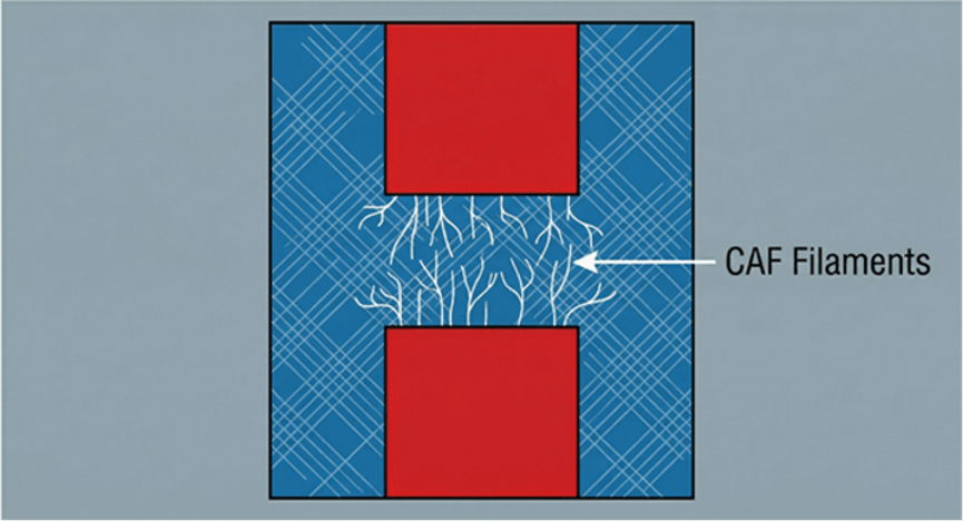
Figure 3: Conductive anodic filament growth
One of the most insidious categories of HDI failure is problems that pass all validation tests but fail after the product has been in use for a long time. These problems usually stem from slowly developing degradation mechanisms that do not cause immediate failure but eventually push the system beyond the limits for reliable operation.
Conductive anodic filament growth:
This is an electrochemical process in which conductive copper filaments grow along glass fiber interfaces in the presence of bias voltage and moisture. HDI designs have tight via spacing and thin dielectric layers, shortening the bridging distance required for these filaments to grow and form a short circuit. The growth rate of conductive anodic filaments depends on moisture exposure, bias voltage, and material sensitivity. What makes this problem frightening is that these conductive filaments may take months or years to bridge the gap between conductors.
Slow crack propagation:
A microvia interface with marginal integrity may pass initial thermal cycling tests, but cracks slowly propagate under actual operating stress. The microvia may function normally for a long time until cumulative crack growth causes intermittent or permanent failure.
Electrochemical migration:
Similar to conductive anodic filaments, in the presence of ionic contaminants and moisture, electrochemical migration causes metal dendrites to grow between conductors under bias voltage. Flux residue, fingerprints, or environmental contamination can all provide the ionic species needed to initiate migration. Time to failure depends on multiple factors, such as contamination level, moisture exposure, and conductor spacing. In aggressive HDI geometries, these factors are increasingly common and prominent, so they cannot be ignored.
Solder joint fatigue at HDI interfaces:
Via-in-pad designs place solder joints directly above filled microvias. If the microvia fill is not completely flat, or if the fill material has a different coefficient of thermal expansion from the surrounding copper, the solder joint experiences greater stress than a BGA solder joint on a solid copper pad. This accelerates solder joint fatigue, especially in high-reliability applications that must withstand longer thermal cycling tests.
Design for Long-Term Reliability
Preventing these deeper failure modes requires going beyond standard design rules and qualification test procedures and taking further measures:
Material selection: Select materials that have been validated for the number of lamination cycles required by the design, and confirm that the material's resistance to conductive anodic filament growth matches the conductor spacing and operating environment in the design.
Copper balance: Ensure that copper density is balanced across the entire board and between layers to promote uniform resin flow and minimize warpage that causes stress concentration.
DFM analysis: Use DFM tools to flag resin deficiency risks, annular ring violations, and other HDI-specific issues before releasing the design to manufacturing.
Extended qualification testing: For high-reliability applications, consider extending thermal cycling test counts beyond standard rules and incorporating moisture exposure to accelerate exposure of latent failure mechanisms.
Cleanliness specifications: Specify and verify ionic cleanliness levels suitable for HDI geometries and operating environments.
HDI technology enables design capabilities that traditional methods cannot achieve. To fully realize these capabilities without sacrificing long-term reliability, it is necessary to comprehensively understand various failure mechanisms and proactively take preventive measures during the design stage, with particular attention to subtle failure mechanisms. Click the image below to read the design guide and fully master the complete workflow guide from stack-up to sign-off.