Excellent PCB design is reflected not only in electrical performance indicators, but also in EMC performance and anti-interference capability. One of the most important factors determining PCB indicators is PCB grounding design.
Excellent PCB design is reflected not only in electrical performance indicators, but also in EMC performance and anti-interference capability. One of the most important factors determining PCB indicators is PCB grounding design.
According to signal types, grounding can be divided into analog ground and digital ground; according to different circuit modules, it can be divided into audio ground, image ground, RF ground, AC power ground, DC power ground, etc.; according to the purpose of the ground, it can be divided into signal return ground, filter grounding, shield grounding, protective grounding, reference ground plane, and so on.
In PCB design, how to reduce ground impedance, equalize the potential between different ground planes, balance ground separation and reference ground plane integrity, and minimize the area of signal return paths after crossing separations will be analyzed and illustrated one by one below.
I. Minimizing Loop Area Through PCB Grounding Design
At low signal frequencies, the signal return mainly follows the path of minimum resistance, i.e., the geometric shortest path. When the signal reaches a certain frequency (F≥1MHz), the signal return is mainly concentrated along the path of minimum inductance, and the return current mainly flows back under the printed trace. The dashed line in the figure indicates the signal return.
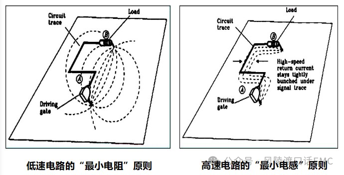
At high signal rates, regardless of whether the signal is close to the power plane or the ground reference plane, the signal return current always flows back along the adjacent reference plane.
1.1 Loop Antenna Effect on PCB
A rapidly changing current loop on a PCB acts like a small loop antenna, which radiates electromagnetic fields outward (a differential mode radiation method). The intensity of the radiated electromagnetic field is proportional to the square of the current I in the loop, the loop area A, and the current frequency. Similarly, the signal loop (small loop antenna) on the PCB will also receive the rapidly changing electromagnetic fields around it and generate interference currents.
When common-mode current exists on the cables entering and exiting the PCB, common-mode radiation will be generated. The intensity of the radiated electric field is proportional to the magnitude of the common-mode current, the frequency of the common-mode current, and the length of the line. At the same time, it will also cause common-mode interference to the circuits on the PCB.
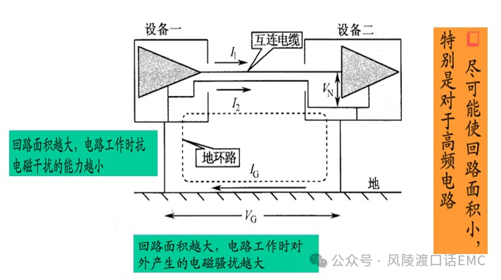
Especially for high-frequency circuits, the larger the loop area, the weaker the circuit's anti-electromagnetic interference capability during operation, and the greater the electromagnetic disturbance generated by the circuit to the outside. Therefore, the loop area should be minimized as much as possible.
1.2 PCB Design for Minimizing Current Loop Area
Minimizing the signal loop area is a very economical and effective measure to improve EMC performance. The PCB design for minimizing the current loop area uses the principle of magnetic flux cancellation to suppress the emission of spatial electromagnetic fields. The design for minimizing PCB current loop area first involves identifying the current loops of interference sources in the circuit (mainly high-frequency current loops); second, analyzing how to design the PCB for the current loops of interference sources to minimize the loop area; and finally guiding PCB Layout engineers in PCB design.
Example: PCB Design for Minimizing Buck DC-DC Current Loop Area
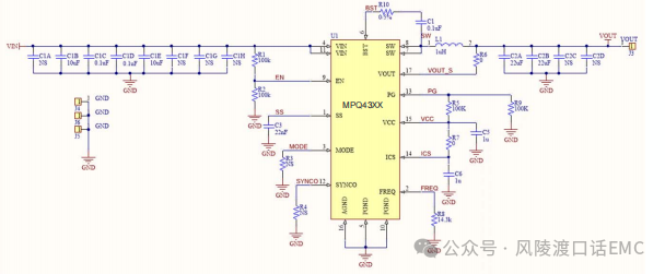
Step 1: Identify the current loops of the interference source
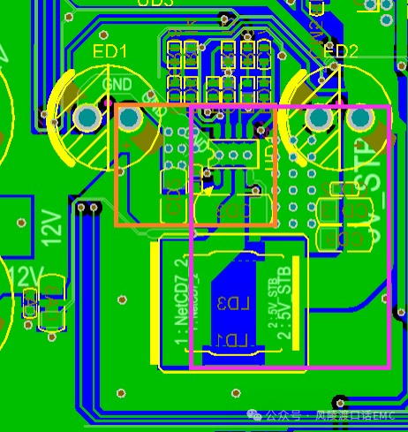
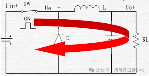
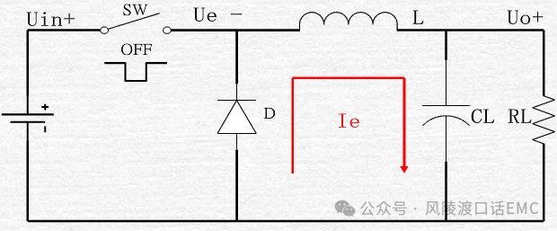
Through analysis, the main current loops of Buck DC-DC are the turn-on loop and the turn-off loop (freewheeling loop), as shown in the figure.
Step 2: Analyze the current loops
For the turn-on loop, the positive pole of the input high-frequency filter capacitor is close to the power pin, and the ground terminal of the filter capacitor is immediately adjacent to the positive pole of the freewheeling diode. For the freewheeling loop, the positive pole of the output high-frequency bypass capacitor is connected to the output pin of the SMD filter inductor, and the ground terminal of the filter capacitor is immediately adjacent to the positive pole of the freewheeling diode. Only through the above PCB design methods can the minimization of the high-frequency loop area of the input and output be achieved.
Step 3: Implement the PCB design for minimizing current loop area
Note: In double-layer board design, the ground terminals of the input and output filter capacitors, the ground terminal of the freewheeling diode, and the ground of the DC-DC IC should be on the same layer, and the connections between them should maintain the minimum impedance, with reference to the Layout as shown in the above figure.
1.3 PCB Design of Signal Return Paths
In multi-layer PCB design, the signal return path is along the bottom reference plane (power plane & reference ground plane) back to the source; in double-layer PCB design, the signal return path can either follow the bottom reference plane or use the ground lines on both sides of the signal as the current return path; in single-layer PCB design, the signal preferably uses the ground lines wrapped on both sides for return, or can return along the nearby metal plane through parasitic capacitance.
Multi-layer board signal return path PCB design
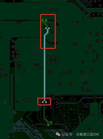
The optimal design for multi-layer PCB is that the signal return path returns to the source along the bottom reference plane (power plane & reference ground plane). During PCB design, the situation where the lower reference plane crosses the separation should be avoided, as shown in the above figure.
When the crossing of the lower reference plane by the signal is inevitable in multi-layer PCB design, accompanying ground lines can be added on both sides of the signal routing to provide a return path for the signal. Coupling capacitors can also be used for bridging at the edge where the reference plane crosses the separation.
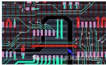
In multi-layer PCB design, the signal sometimes inevitably needs to change layers, and the reference plane also inevitably needs to change layers. If the reference plane changes layers but the attribute remains unchanged, it is only necessary to add ground vias on both sides of the signal layer-changing via to accompany the reference plane layer change. If the attribute of the reference plane changes (from reference ground plane to reference power plane), a bridging capacitor should be added on both sides of the signal layer-changing via to connect the two reference planes with different attributes, as shown in the above figure.
Double-layer board signal return path PCB design
Due to the limitation of PCB layers in double-layer board design, it is difficult to ensure a complete reference plane to provide a return path for the signal. Therefore, in double-layer board design, the ground lines on both sides of the signal are usually selected as the return path. This design method should pay attention to the equipotential problem between the wrapped ground lines on both sides and the reference ground plane. If there is a potential difference between the wrapped ground lines and the reference ground plane, a new common-mode current interference will be generated, leading to serious radiation emission problems.
When selecting the wrapped ground lines on both sides of the signal as the signal return path, attention should also be paid to the integrity of the wrapped ground lines from the source end to the SINK end. When the bottom layer of the signal has a serious cross-separation, the equipotential of the ground lines before and after the cross-separation, and the ground lines of the cross-separation part and the reference ground plane must be ensured.
1.4 Grounding Design of Chip Power Supply Filter Capacitors
The higher the integration of the chip and the more powerful the function, the more complex the power supply design. The reliability of the chip power supply design determines the stability of the system operation. The filtering and decoupling design of the chip power supply is one of the important factors affecting radiation emission, and the stability of the power supply voltage is one of the important factors leading to ESD problems.
For the grounding design of the filter capacitors and decoupling capacitors of the chip power supply, the following design rules should be followed:
- The ground terminal of the chip filter capacitor should be directly connected to the reference ground plane through a via, avoiding connection to the wrapped ground lines on both sides of the terminal signal (double-layer board) to prevent the potential fluctuation of the signal wrapped ground lines from causing the fluctuation of the chip power supply voltage and abnormal chip operation due to undervoltage.
- The chip power supply should be as far away as possible from the external electrostatic discharge test terminal, and the ground terminal of the filter capacitor should also avoid connection to the top layer ground of the electrostatic discharge test terminal shell, to prevent the ground potential fluctuation during electrostatic discharge from causing the fluctuation of the chip power supply voltage and abnormal chip operation due to undervoltage (also to avoid the chip power supply noise radiating outward through the terminal connection line).
- The ground terminal of the chip filter capacitor should be directly connected to the reference ground plane through a via, avoiding connection to the wrapped ground lines on both sides of the internal interconnection socket signal (double-layer board), especially directly to the ground pin of the internal interconnection socket, to prevent the chip power supply noise from coupling to the internal interconnection line through the filter capacitor and radiating outward by means of the cable.
- The ground terminals of the filter capacitors for the power supply of different chip modules should be grounded to the reference ground plane through separate vias, avoiding the common ground via grounding of filter capacitors for different power supplies to prevent power supply noise crosstalk caused by the common via.
Summary of chip power supply filter grounding design
In addition to following the above conventional constraints, the grounding design of the chip power supply filter capacitor should also avoid the filter capacitor being connected to the reference ground plane through a long PCB trace; and the high-frequency loop coupling formed after filtering by the filter capacitors for the power supply of different chip modules.
1.5 Grounding Design of External Terminal Connectors
External terminal connectors are the test points for electrostatic discharge and also the main targets for radiation testing. Therefore, the grounding design of external terminal connectors is an important support for the smooth passing of ESD testing and radiation testing.
The following design rules should be followed for the grounding design of external terminal connectors:
- The ground pin of the metal shell of the external terminal is separated from the chip filter ground on the top layer, and the ground terminal of the chip filter capacitor is grounded to the bottom ground plane through a separate via.
- When the signal routing passes under the external terminal on the top layer, the distance between the top layer ground of the external terminal and the signal routing should be ≥30mil to prevent electrostatic discharge interference from coupling to the signal routing on the top layer and causing ESD problems.
- The internal signal ground of the external terminal is separated from the shell ground of the external terminal on the top layer to prevent the signal ground fluctuation caused by the electrostatic discharge process and signal transmission errors.
- The peak of the tin-free pad of the external terminal signal should avoid facing the external terminal ground to prevent peak discharge between the ground plane and the signal during electrostatic discharge, leading to ESD problems.
- When the direct chip or chip power supply routing is close to the external terminal routing, the distance between the external terminal ground plane and the direct chip routing should be kept ≥30mil to prevent ESD problems.
1.6 Grounding Design of Signal Wrapped Ground Lines
In double-layer board design, the wrapped ground lines on both sides of the signal are mainly used to provide a return path for the signal and isolate crosstalk between signals. In multi-layer board design, they are mainly used to isolate crosstalk between signals or provide return bridging for signals crossing separations. Based on the functional purpose of the wrapped ground lines and combined with the needs of immunity testing and radiation emission testing, the grounding design of the wrapped ground lines should follow the following rules:
- The signal wrapped ground lines shall be prohibited from being directly connected to the ground pin of the external terminal (especially the pin for air discharge testing) on the top layer, to prevent electrostatic discharge interference from passing from the ground pin to the wrapped ground lines and interfering with the sensitive signals on both sides of the wrapped ground lines.
- The wrapped ground lines serving as the signal return path should completely accompany the signal routing from the source end to the receiving end to prevent a large signal return area caused by incomplete wrapped ground lines and serious radiation problems.
- The wrapped ground lines providing shielding for sensitive signals or strong interference signals should maintain the equipotential of the entire trace with the reference ground plane to prevent poor isolation effect or even crosstalk caused by high impedance of the wrapped ground lines (at high frequencies).
- When the wrapped ground lines serving as the signal return path cross a separation, the wrapped ground lines before and after the cross-separation should maintain equipotential with the reference ground plane to prevent common-mode current generated by ground potential difference and serious radiation problems.
1.7 Separation Design of PCB Reference Ground Plane
We know that a complete reference ground plane can provide a low-impedance path for signal return. As mentioned earlier, crosstalk of common ground loops is likely to occur when different signals share a return path. When the PCB area is limited, we usually adopt the method of reference ground plane separation to solve the problem of common ground loop interference between different signals. The principles to be followed for the separation of the reference ground plane are: keep complete if possible, separate the return paths of strong and weak signals, and the separation should take into account the electrostatic current discharge path.
1.8 Grounding Design of PCB Screw Holes
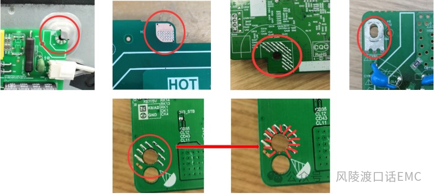
The main functions of PCB grounding screw holes are: first, to establish an equipotential body between the PCB board and the metal backplane, reduce the high-frequency loop area, reduce the ground plane noise current, and cut off the noise coupling path; second, to provide a low-impedance discharge path for electrostatic current, shunt the electrostatic current, and reduce the electrostatic discharge interference to the components and signals on the PCB board.
The number, placement position, and pad design of the grounding screw holes are the main factors determining whether the grounding screw holes can achieve the minimum grounding impedance design, so they should be paid close attention to in PCB design.
Case Analysis of Reliable Grounding Design of Screw Holes
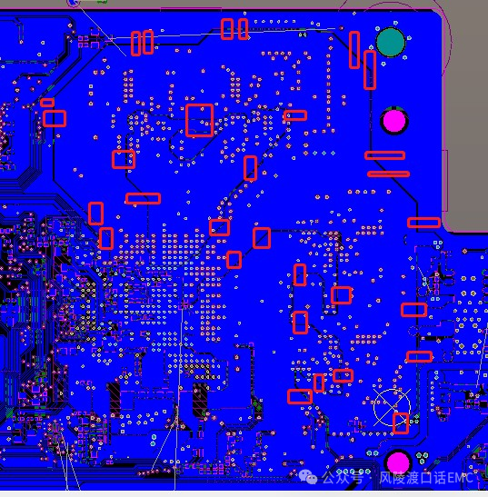
Case 1: Since the grounding screw is locked to the screen metal backplane through the plastic hole of the AC socket, the contact area between the convex hull of the screen metal backplane and the board card grounding screw hole is small, the grounding impedance is high at high frequencies, the Y capacitor grounding is poor, and the radiation test seriously exceeds the standard.
Case 2: Due to the diversity of the locking methods of the whole machine board card, the design of the grounding screw hole should select an appropriate grounding method according to the actual production locking method of the whole machine, as long as it can achieve the purpose of electrostatic current shunting and reducing the high-frequency loop area.
II. Shielding Grounding Design
2.1 Definition of Shielding
Shielding is to use a box, shell, plate and other structural forms made of conductive or magnetic materials to limit the electromagnetic interference field within a certain space range, so that the interference field is greatly attenuated when passing through the shield, thereby suppressing the interference of the electromagnetic interference source on related equipment or space.
Shielding is one of the powerful measures to suppress electromagnetic interference sources. It is divided into electric field shielding, magnetic field shielding and electromagnetic field shielding according to the focus of shielding. Electric field shielding: shielding of electrostatic field or alternating electric field, preventing or suppressing parasitic capacitance coupling, and isolating electrostatic field or alternating electric field interference. Magnetic field shielding: used to prevent magnetic induction, suppress parasitic inductance coupling, and isolate magnetic field interference. Electromagnetic field shielding: used to prevent and suppress high-frequency electromagnetic fields (electromagnetic waves).
The performance of the shield design is reflected by the Shielding Effectiveness (SE) index. Shielding effectiveness is the ratio of the electric (magnetic) field strength at a certain point in space before and after shielding, usually expressed in decibels:
SE=20lgE1/E2 dB
2.2 Electric Field Shielding and Grounding Design
From the perspective of the field, the essence of electric field shielding is that the electric field lines emitted by the interference source are terminated in the shield, cutting off the coupling path of the interference source or the connection with sensitive equipment. From the perspective of the circuit, the shield serves to avoid or reduce the distributed capacitance coupling between the interference source and the sensitive equipment.
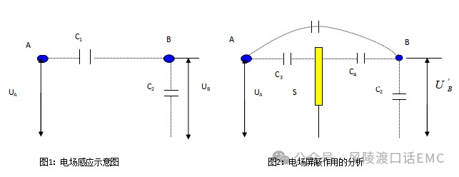
Design principles of electric field shielding:
- Any metal can be used for electric field shielding, and there is no strict requirement on the thickness of the metal, as long as it has sufficient strength.
- The shield should be as close as possible to the circuit, components and PCB routing that need to be shielded, and the shield should be well grounded.
- The shape of the shield has the most direct impact on the shielding effect. It is best if the shield can be made into a fully enclosed metal box, but it should be determined according to the specific situation in practical applications.
- Single-point grounding is usually sufficient for low-frequency electric field shielding, such as switching transformers and PFC inductors. For high-frequency electric field shielding, it is necessary to ensure the low impedance of the grounding point, and multi-point grounding is usually adopted, such as the shielding of the main chip heat sink and the shielding of the silicon high-frequency head chip. Multi-point grounding can reduce the grounding impedance and make the shield and the ground form an equipotential body.
2.3 Magnetic Field Shielding
Magnetic field shielding can be divided into low-frequency magnetic field shielding and high-frequency magnetic field shielding. A magnetic field is generated around any current-carrying conductor or coil, and the magnetic field changes with the change of the conductor current. This changing magnetic field often causes interference to the surrounding electronic circuits or sensitive components. Strong signal loops are easy to form magnetic field radiation, and weak signal loops are susceptible to interference from the surrounding alternating magnetic fields.
2.3.1 Principle of Low-Frequency Magnetic Field Shielding
The high magnetic permeability characteristics of ferrite materials, permalloy and silicon steel sheets are used to shunt the interference magnetic field. The higher the magnetic permeability, the smaller the magnetic resistance, and the magnetic flux mainly passes through the high magnetic permeability material. If there is a magnetic field path with high magnetic permeability in the magnetic field, the part of the magnetic flux passing through the surrounding air is greatly reduced, so that the magnetic field interference in the surrounding space is also greatly reduced, which objectively plays a role in magnetic field shielding.
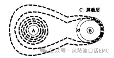
2.3.2 Principle of High-Frequency Magnetic Field Shielding
The principle of high-frequency magnetic field shielding is that the shield uses the eddy current reverse magnetic field generated by the electromagnetic induction phenomenon to repel the original interference magnetic field to achieve the shielding purpose. The shielding material is a good conductor with low resistivity, such as copper and copper-plated silver.
According to Faraday's law of electromagnetic induction, the induced electromotive force generated by a closed loop is equal to the rate of change of the magnetic flux passing through the loop. The induced electromotive force is accompanied by an induced current, and the magnetic flux generated by the induced current will hinder the change of the original magnetic flux, with the opposite direction to the original magnetic flux, i.e., the reverse magnetic field.
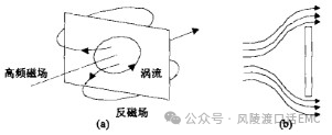
Design principles of magnetic field shielding:
- The selection of high magnetic permeability materials is very important for low-frequency magnetic field shielding. The magnetic permeability changes with the change of the external magnetic field strength. When the external magnetic field strength is low, the magnetic permeability increases with the increase of the magnetic field strength, and when the external magnetic field strength exceeds a certain limit, the magnetic permeability drops sharply. At this time, the magnetic conductive material is magnetically saturated, which also means that the material loses its magnetic shielding performance at the same time. The higher the magnetic permeability, the easier it is to saturate, so selecting a magnetic conductive material with sufficient magnetic permeability and saturation characteristics is the key to low-frequency magnetic field shielding.
- The shielding material for high-frequency magnetic field needs to be a good conductor to reduce the eddy current impedance and reduce heating and loss. At the same time, gaps in the direction perpendicular to the eddy current should be avoided as much as possible to prevent hindering the flow of eddy current and affecting the shielding effectiveness. Due to the skin effect of high-frequency current, the high-frequency shielding box does not need to be too thick.
- In addition, whether the shield is grounded or not does not affect the shielding effect, but since electric field shielding must be grounded, grounding the shield will have the dual effect of electric field shielding and high-frequency magnetic field shielding at the same time.
2.4 Electromagnetic Field Shielding
Electromagnetic field shielding is divided into near-field shielding and far-field shielding. For the near field, if the radiation source is high voltage and small current, the main consideration is electric field interference; if the radiation source is low voltage and large current, the main consideration is magnetic field interference. In the far field, the electric field and magnetic field are perpendicular to each other but in the same phase, radiating energy to all directions in space in the form of electromagnetic waves.
Electromagnetic wave shielding mainly uses the incident loss and reflection loss generated when electromagnetic waves pass through metal and other shielding materials to attenuate the energy of electromagnetic waves. The large attenuation of low-frequency electromagnetic waves depends on the reflection loss, while the attenuation at high frequencies is mainly due to the absorption loss. The selection of shielding materials has a very important impact on the electromagnetic field shielding effectiveness. Some metals have large absorption loss for electromagnetic waves, such as nickel-steel alloy and permalloy, but they are all expensive. Any metal can be used, and the shielding effectiveness of metal mesh is much worse than that of metal plate, especially at high frequencies. When metal mesh shielding needs to be adopted, double-layer or multi-layer metal mesh shielding is often used.
About Maxipcb
Maxipcb empowers innovators to turn cutting-edge technologies into reality.
We offer one-stop solutions for design, simulation, testing, PCB manufacturing, component procurement and SMT assembly, enabling efficient development, rapid deployment and risk control across the full product lifecycle.Serving the world in communications, industrial automation, aerospace, automotive, semiconductor and beyond, we build a safer, more connected future together.