01. Power supply placement and routing considerations
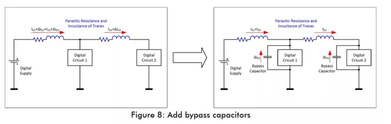
In digital circuits, the current required is often discontinuous, so some high‑speed devices generate surge currents.
If the power traces are very long, these surge currents can create high‑frequency noise, which can be coupled into other signals.
In high‑speed circuits, parasitic inductance, parasitic resistance, and parasitic capacitance inevitably exist. This high‑frequency noise can eventually couple into other circuits. Moreover, the parasitic inductance reduces the maximum surge current that the trace can handle, leading to some voltage drop and possibly causing the circuit to malfunction.
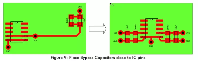
Therefore, it is particularly important to add bypass capacitors in front of digital devices. Larger capacitors are limited in their energy‑delivery rate, so it is common to use a large capacitor in parallel with a small one to cover the full frequency range.
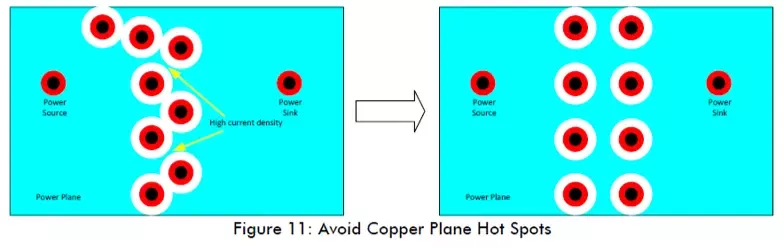
Avoiding hot spots: Signal vias create voids in the power and ground planes. Improper placement of vias can increase current density in certain areas of the power or ground planes – these areas are called hot spots. Therefore, when placing vias, we must try to avoid such situations, lest the planes be fragmented and eventually cause EMC problems. The best way to avoid hot spots is to distribute vias in a grid‑like pattern; this ensures uniform current density, prevents plane isolation, keeps return paths short, and avoids EMC issues.
02. Trace bending styles
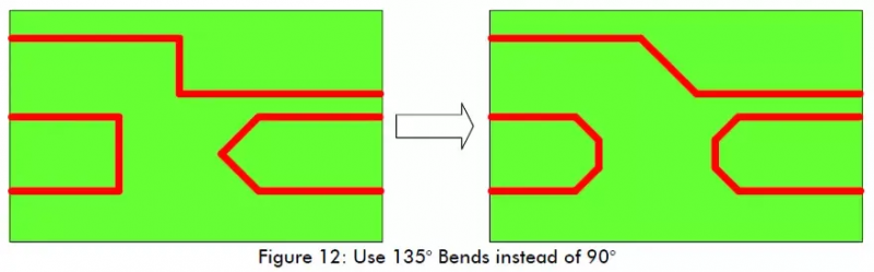
When routing high‑speed signal lines, bends should be avoided as much as possible. If bending is unavoidable, never use sharp or right‑angle bends; instead, use obtuse‑angle bends.
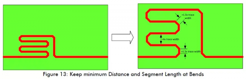
In high‑speed signal routing, we often use serpentine traces to achieve length matching. Serpentine traces are also a form of bending. The trace width, spacing, and bending style should be chosen appropriately; the spacing should meet the 4W/1.5W rule.
03. Signal proximity
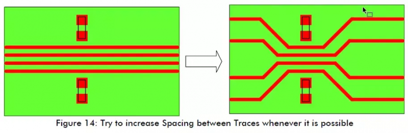
If high‑speed signal lines are too close to each other, crosstalk can easily occur. Sometimes, due to layout constraints or board dimensions, the distance between high‑speed signal lines ends up smaller than our minimum requirement. In such cases, we should increase the spacing as much as possible in the bottleneck areas. If space permits, always increase the spacing between two high‑speed signal lines.
04. Trace stubs
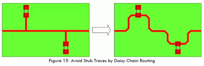
A long stub behaves like an antenna and, if not handled properly, can cause serious EMC problems. Stubs also cause reflections, reducing signal integrity.
Stubs are most commonly created when adding pull‑up or pull‑down resistors on high‑speed signal lines. A common way to handle stubs is to use daisy‑chain routing.
Experience shows that if a stub is longer than 1/10 of the wavelength, it can act as an antenna and become a problem.
05. Impedance discontinuity
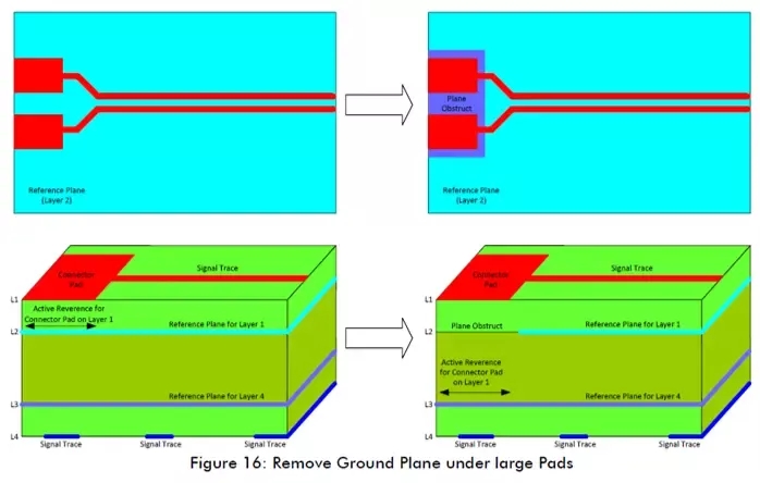
The impedance of a trace generally depends on its width and the distance to the reference plane. Wider traces have lower impedance. The same principle applies to the pads of connectors and components.
When a connector pad is connected to a high‑speed signal line, if the pad is very large while the signal line is very narrow, the large pad presents low impedance and the narrow trace presents high impedance. This creates an impedance discontinuity, which in turn causes signal reflections.
To address this, a common practice is to place a copper‑keep‑out area under the large pad of the connector or component, and on another layer place a reference plane for that pad, thereby increasing the impedance to achieve continuity.
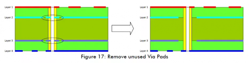
Vias are another source of impedance discontinuity. To minimise this effect, unnecessary copper on inner layers connected to the via should be removed. This can be done during design using CAD tools, or by coordinating with the PCB manufacturer to remove unwanted copper and ensure impedance continuity.
06. Differential signals
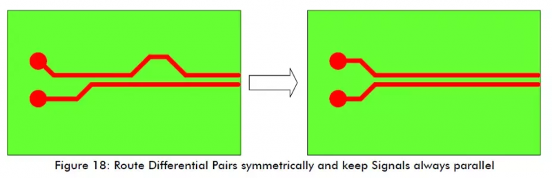
High‑speed differential signal pairs must maintain equal width and equal spacing to achieve the specified differential impedance. Therefore, when routing differential pairs, keep them as symmetrical as possible.
Do not place vias or components between the two lines of a differential pair. Doing so can cause EMC problems and impedance discontinuity.
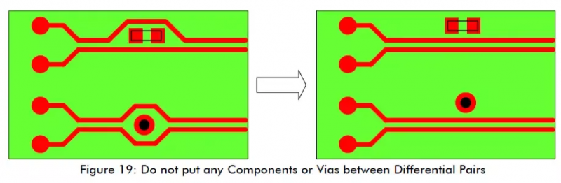
Sometimes, high‑speed differential signals need AC‑coupling capacitors in series. These capacitors should also be placed symmetrically, and their package size should not be too large. It is recommended to use 0402; 0603 is acceptable, but capacitors of 0805 or larger, or tandem capacitors, should be avoided.
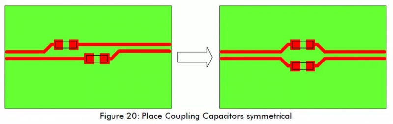
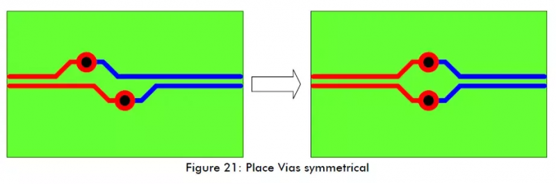
In general, vias create significant impedance discontinuity, so for high‑speed differential pairs, minimise the number of vias. If vias are necessary, place them symmetrically.
07. Length matching
For many high‑speed signal interfaces, such as buses, the arrival times and skew between signal lines must be considered.
For example, all data signal lines in a high‑speed parallel bus must have their arrival times kept within a certain skew tolerance to ensure consistent setup and hold times. To meet this requirement, length matching is necessary.
For high‑speed differential pairs, the skew between the two lines must be strictly controlled; otherwise, communication may fail. To achieve this, serpentine traces can be used to match the lengths and meet the skew requirements.
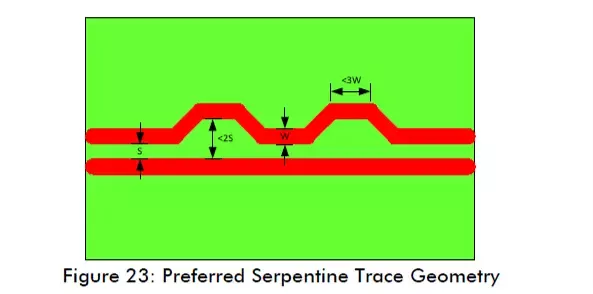
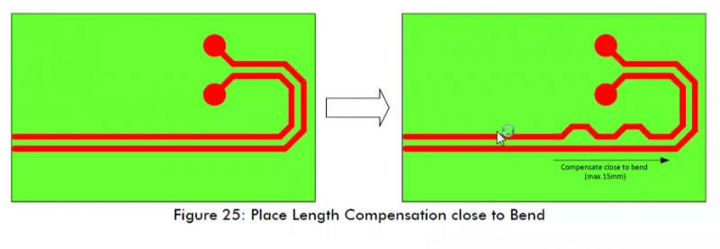
Serpentine traces should generally be placed at the source of the length mismatch, not at the far end. Placing them at the source ensures that the positive and negative signals of the differential pair are synchronously transmitted for most of the path.
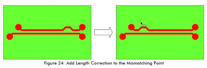
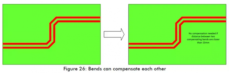
Trace bends are one source of length mismatch. For bends, length compensation should be placed close to the bend (≤ 15 mm).
If there are two bends and the distance between them is < 15 mm, the mismatches from each bend will compensate for each other, so no additional length‑matching is needed.
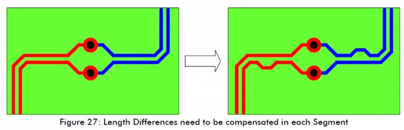
For different sections of high‑speed differential pairs, each section should be length‑matched independently. Vias, AC‑coupling capacitors, and connectors split the differential pair into separate sections, so special attention is required – each section must be matched separately. This is because many EDA tools only check the overall length mismatch during DRC.
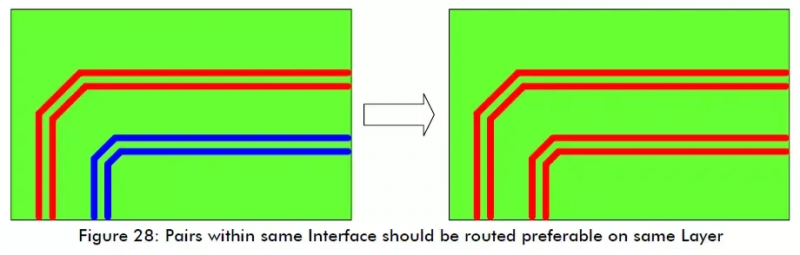
For interfaces such as LVDS display devices, there may be multiple differential pairs with very strict timing requirements and very small skew tolerances. For such differential pairs, it is generally recommended to perform compensation on the same layer, because signal propagation speeds differ between layers.
Some EDA software calculates the trace length including the portion inside the pad. If length compensation is performed based on that value, the actual result may still have a mismatch. Therefore, special attention is needed when using such EDA tools.
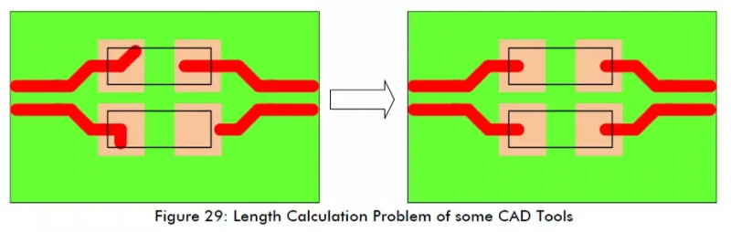
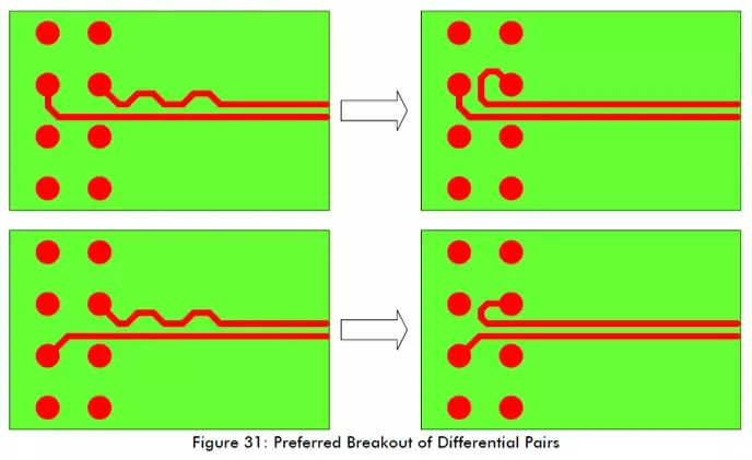
Whenever possible, choose symmetrical breakout routing to avoid the need for serpentine traces solely for length matching.
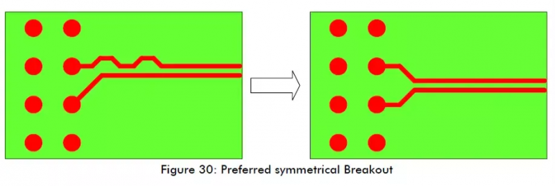
If space permits, add a small loop at the source of the shorter differential trace to compensate, rather than using serpentine traces.