In the application design of DC-DC chips, a rational PCB layout is crucial for the chip to exhibit its optimal performance. An unreasonable PCB layout can degrade chip performance—such as reduced linearity (including input and output linearity), lower load capacity, unstable operation, increased EMI radiation, and higher output noise. In more severe cases, it may even directly cause chip damage.
In the application design of DC-DC chips, a rational PCB layout is crucial for the chip to exhibit its optimal performance. An unreasonable PCB layout can degrade chip performance—such as reduced linearity (including input and output linearity), lower load capacity, unstable operation, increased EMI radiation, and higher output noise. In more severe cases, it may even directly cause chip damage.
The datasheets of general DC-DC chips all specify corresponding PCB layout requirements and provide layout schematics. This article takes a synchronous BUCK chip as an example to briefly explain the key points of PCB Layout design in the application of DC-DC chips.
1 Focus on the High-Current Paths of Chip Operation
A critical principle for DC-DC chip layout is to
minimize the area of the switching high-current loop as much as possible. As shown in the BUCK topology structure below, there are two high-current loops during the chip's switching process: the red one is the input loop, and the green one is the output loop. Each current loop can be regarded as a loop antenna that radiates energy outward and causes EMI issues, with the radiation intensity being proportional to the loop area.
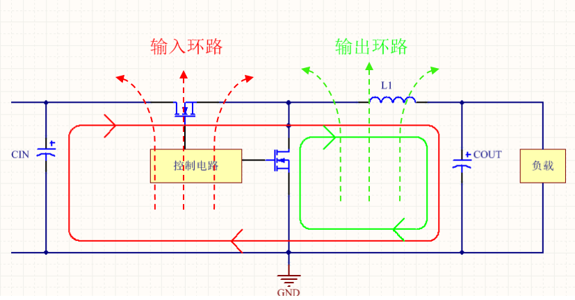
Note: When the chip pin configuration makes it impossible to minimize both the input and output loops simultaneously, for BUCK chips, priority should be given to optimizing the wiring of the input loop. This is because the current in the output loop is continuous, while the current in the input loop is abrupt, generating a large di/dt and posing a higher risk of EMI problems. For BOOST chips, the wiring optimization of the output loop should be prioritized instead.
2 Configuration of Input Capacitors
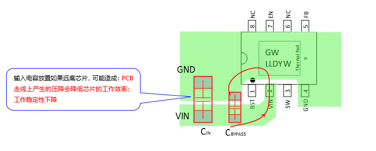
For BUCK chips, to minimize the input loop, the input capacitor should be placed as close to the chip pins as possible.
- To enhance the filtering effect of the capacitor, the power supply should pass through the input capacitor first before entering the chip interior.
- The large-capacity capacitor used for CIN generally has poor frequency characteristics, so it should be paralleled with a high-frequency decoupling capacitor CBYPASS with good frequency characteristics.
- For low current-capacity power supplies (IO≤1A), the required capacitance is also smaller, so a single ceramic capacitor can sometimes serve as both CIN and CBYPASS.
Improper placement of the input capacitor (too far from the chip) may cause:
- Voltage drop on the PCB traces, reducing the chip's operating efficiency;
- Degraded operational stability.
3 Configuration of Inductors
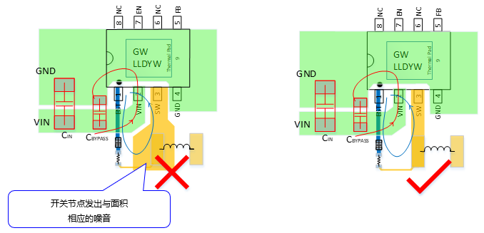
For BUCK chips, to minimize the input loop, the inductor should be placed close to the SW pin of the chip.
- Use copper pouring for trace routing to reduce parasitic inductance and resistance.
- The SW node should handle high current with the smallest possible area to prevent the enlarged copper foil from acting as an antenna and increasing EMI.
- Avoid routing sensitive signal lines near the inductor.
- For the bootstrap circuit, place it as close to the SW pin as possible to shorten the entire high-frequency current path.
Reference: Correlation of PCB Trace Width, Copper Thickness and Carrying Current (at 10℃ Temperature Rise)
| Trace Width (mm) |
Copper Thickness 1oz (0.035mm)
Current (A) |
Copper Thickness 1.5oz (0.05mm)
Current (A) |
Copper Thickness 2oz (0.07mm)
Current (A) |
| 0.15 |
0.2 |
0.5 |
0.7 |
| 0.2 |
0.55 |
0.7 |
0.9 |
| 0.3 |
0.8 |
1.1 |
1.3 |
| 0.4 |
1.1 |
1.35 |
1.7 |
| 0.5 |
1.35 |
1.7 |
2 |
| 0.6 |
1.6 |
1.9 |
2.3 |
| 0.8 |
2 |
2.4 |
2.8 |
| 1 |
2.3 |
2.6 |
3.2 |
| 1.5 |
3.2 |
3.5 |
4.2 |
| 2 |
4 |
4.3 |
5.1 |
| 2.5 |
4.5 |
5.1 |
6 |
| 3 |
5 |
5.5 |
6.4 |
| 4 |
5.4 |
6.2 |
7.9 |
| 5 |
5.6 |
7.3 |
9.3 |
| 8 |
7.9 |
10.3 |
13.1 |
| 10 |
9.3 |
12 |
15.4 |
4 Configuration of Output Capacitors
In a step-down converter, the output current is smoothed due to the series inductor connected to the output.
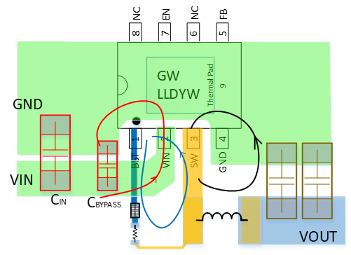
- The output capacitor should be placed close to the inductor.
5 Wiring of the Feedback Path
- The voltage divider resistors in the FB feedback network typically use resistances of the kΩ, 10 kΩ, or even hundreds of kΩ range. Higher resistance values make the network more susceptible to interference, so it should be placed far away from various noise sources (e.g., inductors, SW nodes, freewheeling diodes).
- The signal ground of the FB and COMP pins should be isolated as much as possible from the power ground carrying large currents, and then connected at a single point. Do not let the ground of large-current signals interfere with the ground of small-signal currents.
- The voltage divider resistors of the FB should sample from VOUT, and the sampling point should be close to the output capacitor to obtain a more accurate actual output voltage value.

About Maxipcb
Maxipcb empowers innovators to turn cutting-edge technologies into reality.
We offer one-stop solutions for design, simulation, testing, PCB manufacturing, component procurement and SMT assembly, enabling efficient development, rapid deployment and risk control across the full product lifecycle.
Serving the world in communications, industrial automation, aerospace, automotive, semiconductor and beyond, we build a safer, more connected future together.