To ensure the performance and manufacturing feasibility of printed circuit boards (PCBs), standardized inspections are generally conducted, including electrical rules, wiring and layout, component packaging, mechanical dimensions and positioning, as well as production, manufacturing and assembly checks, EMC/EMI compliance, DFM/DFA evaluation, and document integrity. These inspections reduce late-stage manufacturing defects and improve product stability and reliability.
To ensure the performance and manufacturing feasibility of printed circuit boards (PCBs), standardized inspections are generally conducted, including electrical rules, wiring and layout, component packaging, mechanical dimensions and positioning, as well as production, manufacturing and assembly checks, EMC/EMI compliance, DFM/DFA evaluation, and document integrity. These inspections reduce late-stage manufacturing defects and improve product stability and reliability.
In PCB design, layout and wiring are key steps that determine the overall board performance, reliability and manufacturing costs. This article focuses on an overview of the relevant check items for these two aspects.
Layout Inspection
1. Netlist Import
Import the netlist generated from the latest schematic into the PCB to ensure consistency between the schematic and PCB design.
2. Outline Dimensions
- Confirm the outline drawing is the latest version.
- Confirm the outline drawing accounts for non-routing areas, transmission edges, baffle edges, panelization and other issues.
- Confirm the PCB template is the latest version.
- Compare with the outline drawing to verify the marked dimensions and tolerances of the PCB are correct, and the definitions of plated and non-plated holes are accurate.
- Confirm the non-routing areas on the outline drawing are reflected in the PCB design.
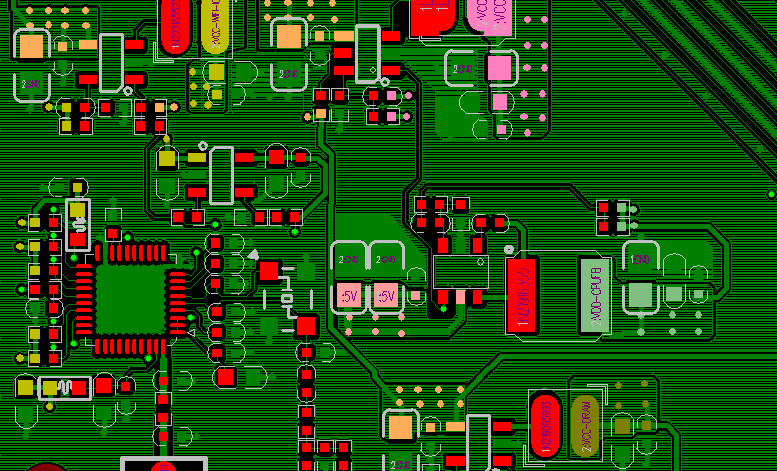
3. Component Layout
- Verify that digital and analog circuits are separated and the signal flow is rational.
- Check the rationality of clock device layout.
- Check the rationality of high-speed signal device layout.
- Ensure termination devices are properly placed (series resistors at the signal driver end, other termination types at the signal receiver end).
- Verify the quantity and position of decoupling capacitors for IC devices are reasonable.
- Maintain proper component spacing: ≥1mm for ICs, ≥3mm for BGAs.
- Check the rationality of the layout and relative positions of protection devices (e.g., TVS, PTC).
- Design the overall power supply layout to ensure a single, non-circuitous power flow direction.
- Place components that may affect EMC testing in accordance with design guidelines or proven experience (e.g., the panel reset circuit should be close to the reset button).
- Mount heavy components near PCB support points or edges to reduce PCB warpage.
- Keep heat-sensitive components (including liquid dielectric capacitors, crystal oscillators) away from heat sources such as high-power components and heat sinks.
- Ensure component heights comply with the outline drawing requirements.
- Within a 5mm range around crimp sockets: no components with height exceeding the socket on the top side; no components or solder joints on the bottom side.
- Arrange test interfaces and LED lights on the side convenient for testing.
- For tall axial through-hole components on the PCB, consider horizontal mounting, reserve horizontal placement space, and design fixing methods (e.g., fixing pads for crystal oscillators).
- For components with metal housings, ensure sufficient clearance to avoid contact with other components or printed traces.
- For motherboards/daughterboards and single boards/backplanes, verify signal correspondence, position alignment, correct connector direction and silkscreen marking.
- Enable place-bound on the TOP and BOTTOM layers to check if DRC errors caused by overlapping are allowed.
- For the wave soldering side, only allow SMDs of the following types: 0603 and larger (inclusive) surface-mount R/C, SOT, SOP (pin center distance ≥1mm).
- On the wave soldering side, SMDs should be placed perpendicular to the PCB transmission direction during wave soldering.
- On the wave soldering side, the shadow effect area is 0.8mm (perpendicular to PCB transmission direction) and 1.2mm (parallel to PCB transmission direction); 2.5mm for tantalum capacitors (judged by pad spacing).
- Confirm 100% of components are placed.
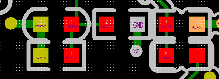
4. Component Packaging
- Print a 1:1 layout drawing to inspect layout and packaging, with confirmation by hardware designers.
- Check component pin order, Pin 1 marking, component polarity marking, and connector direction marking.
- Verify the silkscreen size of component packages is appropriate and component designators comply with standard requirements.
- Check the via pad aperture of through-hole components is suitable and the metallization definition of mounting holes is accurate.
- Ensure the pad width and length of surface-mount devices are appropriate (pad outer margin ≈0.4mm, inner margin ≈0.4mm, width not less than the maximum pin width).
- Distinguish between packages for resistors/capacitors on reflow and wave soldering sides.
- Confirm the package library has been updated (check operation results with viewlog).
Wiring Inspection
1. EMC and Reliability
- Confirm 100% wiring routability.
- Ensure clock lines, differential pairs and high-speed signal lines meet SI constraint requirements.
- Verify impedance consistency of high-speed signal lines across all layers.
- Ensure all types of BUS meet SI constraint requirements.
- Check that interface signals (E1, Ethernet, serial port, etc.) meet relevant requirements.
- Prevent clock lines, high-speed signal lines and sensitive signal lines from crossing reference planes to form large signal loops.
- Ensure power and ground can carry sufficient current (estimation method: 1A/mm line width for 1oz outer layer copper, 0.5A/mm for inner layers, double current for short traces).
- After leading out power/ground lines from chip pads, connect them to power/ground planes nearby with line width ≥0.2mm (8mil), preferably ≥0.25mm (10mil).
- Ensure power and ground planes have no isolated islands or narrow channels.
- Verify the rationality of the design for working ground (digital and analog ground), protective ground, ESD protection and shielding ground on the PCB.
- Check the rationality of the position and connection method for single-point grounding.
- Ensure metal housing devices requiring grounding are properly grounded.
- For polar capacitors (e.g., tantalum capacitors), ensure sufficient connection to power and ground planes; use more than 2 vias for layer transitions if needed.
- No traces, copper foils or vias that may cause short circuits around mounting screws or washers (refer to the structural drawing if available; confirm the required clearance with the structural engineer if not).
- Avoid acute angles and unreasonable right angles on signal lines.
- Minimize the impact of T-type routing stubs during wiring.
- Implement the 3W principle for differential pairs as much as possible, and pay attention to coupling when drilling vias for layer transitions.
- For signal layer wiring on adjacent layers, use perpendicular routing as much as possible; comply with the 3W principle if perpendicular routing is not feasible.
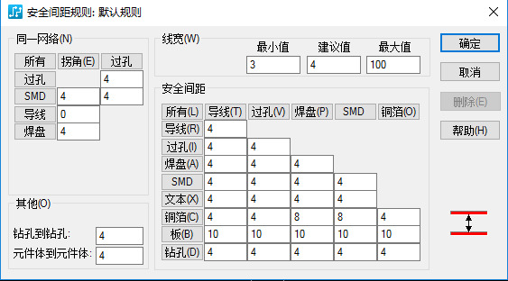
2. Clearance
- Ensure the Spacing rule set meets the minimum clearance requirements.
- Implement the 3W principle as much as possible between different buses and between interference signals and sensitive signals.
- Implement the 3W principle for differential pairs as much as possible.
- Determine the line spacing of differential pairs based on differential impedance calculation and control with design rules.
- For non-plated holes: inner layer clearance to traces/copper foils >0.5mm (20mil), outer layer >0.3mm (12mil); for single board extraction wrench shaft holes: inner layer clearance to traces/copper foils >2mm (80mil).
- Recommended clearance between copper foils/traces and board edges >2mm, minimum 0.5mm.
- Inner layer ground plane copper foil to board edges: 1-2mm, minimum 0.5mm.
- Ensure the 20H principle is implemented as much as possible between the edges of inner layer power and ground planes.
3. Pad Lead-out
- For chip components using reflow soldering, achieve symmetrical lead-out for chip resistors and capacitors as much as possible, and ensure the clines connected to the pads have the same width (not required for components with package >0805 and line width <0.3mm/12mil).
- For SMD chip components with package ≤0805, use a narrow cline transition when connecting to a wider cline to prevent the "tombstoning" defect.
- Lead out traces from both ends of the pads of devices such as SOIC, PLCC, QFP and SOT as much as possible.
4. Vias
- The drilled via aperture should not be less than 1/8 of the board thickness.
- Avoid overly dense via arrangement to prevent large-scale fractures of power and ground planes.
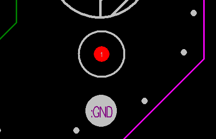
- On the reflow soldering side, do not design vias on pads; the clearance between normally windowed vias and pads >0.5mm (20mil), and the clearance between green oil-covered vias and pads >0.15mm (6mil) (method: enable Same Net DRC to check for errors, then disable it).
- Avoid drilling vias on pads except for large heat-dissipating pads.

5. Non-Routing Areas
- No traces, copper foils or vias that may cause short circuits under metal housing devices and heat-dissipating devices.
- No traces, copper foils or vias that may cause short circuits around mounting screws or washers.
6. Large-Area Copper Foils
- For large-area copper foils on the Top and Bottom layers, use grid copper if there is no special requirement (diagonal grid for single boards, orthogonal grid for backplanes, line width 0.3mm/12mil, spacing 0.5mm/20mil).
- Design component pads in large-area copper foil areas as thermal relief pads to prevent cold soldering; for current-carrying requirements, first widen the thermal relief spokes, then consider full connection.
- Minimize unconnected "dead copper" when laying large-area copper foils.
- Ensure no isolated copper islands exist.
- Keep dynamic copper foils in a smooth state (update to smooth).
- For large-area copper foils, check for illegal connections and unreported DRC errors.
- Avoid full connection between small pads and large copper foils to prevent soldering issues caused by excessive heat dissipation of copper foils; widen the connecting lines for current-carrying requirements.
7. Test Points
- Ensure sufficient test points for all power supplies and grounds (at least one test point per 2A of current).
- Maximize the number of test points.
- Ensure the spacing settings for Test Vias and Test Pins are sufficient.
- Fix the positions of Test Vias and Test Pins.
8. DRC (Design Rule Check)
- Update DRC and check for non-permissible errors.
- Set the Spacing Rule for Test Vias and Test Pins to the recommended distance for DRC checking; if errors still exist, recheck with the minimum distance setting.
9. Fiducial Marks
- Ensure sufficient Mark points in the schematic.
- The three optical fiducial marks should have the same background, with their centers ≥5mm from the board edges.
- For ICs with pin center distance ≤0.5mm and BGA devices with ball pitch ≤0.8mm (31mil), place optical fiducial marks near the component diagonals.
- Isolated optical fiducial marks with no wiring within a 10mm radius should be designed with a protective ring (inner diameter 3mm, ring width 1mm).
10. Solder Mask Inspection
- Confirm all types of pads are correctly windowed.
- Verify that vias under BGAs are processed as green oil plugged vias.
- Ensure all vias except test vias are designed with small windows or green oil plugged.
- Avoid exposed copper and traces in the windowing of optical fiducial marks.
- Check that devices requiring copper foil for heat dissipation or grounding shielding (e.g., power chips, crystal oscillators) have copper foils with correct windowing; devices fixed by solder should have green oil to block large-area solder diffusion.
11. Silkscreen
- Ensure the PCB code (copper lettering) is clear, accurate and placed in compliance with requirements.
- Avoid traces and vias under barcode boxes; check the placement of PCB name and version silkscreen, and ensure no unplugged vias are present underneath.
- Verify no missing component designators and their positions can correctly identify components.
- Ensure component designators comply with company standard requirements.
- Prevent silkscreen from covering copper lettering on the board surface.
- Recommended size for component designators on the silkscreen layer: 20-25mil width, 30-35mil height (adjust appropriately based on board density).
- Standardize the text direction of silkscreen layer components: top layer – left to right, bottom to top; bottom layer – right to left, bottom to top.
- Enable the solder mask to check that characters, Pin 1 marks, polarity marks and direction marks are clearly identifiable (only two text directions allowed on the same layer: up and left).
- Ensure backplanes have correct markings for slot names, slot numbers, port names and sheath directions.
- After generating GERBER files, re-import the silkscreen layer for separate inspection to ensure accuracy.
12. Drill Drawing
- Verify the correctness of PCB board thickness, layer count, silkscreen color, warpage and other technical notes in the Notes section.
- Check the accuracy of layer names, stacking order, dielectric thickness and copper foil thickness in the stack-up drawing; confirm if impedance control is required and the description is accurate. Ensure the layer names in the stack-up drawing are consistent with the GERBER file names.
[Insert Figure: Screenshot of PCB stack-up drawing and drill drawing parameters]
13. Other Items
- Verify the correspondence of plug-in direction markings between motherboards and daughterboards.
- Carefully check and address issues from process feedback.
About Maxipcb
Maxipcb empowers innovators to turn cutting-edge technologies into reality.
We offer one-stop solutions for design, simulation, testing, PCB manufacturing, component procurement and SMT assembly, enabling efficient development, rapid deployment and risk control across the full product lifecycle.Serving the world in communications, industrial automation, aerospace, automotive, semiconductor and beyond, we build a safer, more connected future together.


