When designing complex PCBs, it is essential to make design trade-offs, as these trade-offs result in several factors that influence the design of the PCB Power Distribution Network (PDN).
When designing complex PCBs, it is essential to make design trade-offs, as these trade-offs result in several factors that influence the design of the PCB Power Distribution Network (PDN).
Trade-offs in PCB Power Supply Design
When a capacitor is mounted on a PCB, an additional loop inductance is introduced, which is related to the capacitor's mounting method. The value of the loop inductance is design-dependent, determined by the width and length of the trace from the capacitor to the via, the length of the trace connecting the capacitor to the power/ground plane, the distance between two vias, the via diameter, the capacitor pad, and other factors.
Key Design Points for Reducing Capacitor Loop Inductance
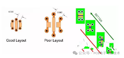
- Place vias as close to the capacitor as possible. Minimize the power/ground via pitch; if feasible, parallel multiple pairs of power/ground vias. For example, place two vias with opposite current polarities as close as possible, and vias with the same current polarity as far apart as possible.
- Use short, wide traces to connect vias to capacitor pins.
- Mount capacitors on the PCB surface (top and bottom layers) as close as possible to their corresponding power/ground planes to reduce the distance between vias. Use a thin dielectric layer between the power and ground planes.
The following analyzes three different design scenarios regarding capacitor mounting and spreading inductance.
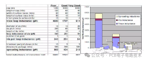
Scenario 1 - Poor Design
- The designer pays no attention to Power Distribution Network (PDN) design.
- Via pitch is not optimized.
- The distance between the power and ground planes is not optimized.
- The trace distance from vias to capacitor pins is long.
For the total loop inductance, the dominant contributor is the routed traces, as the trace length in a poor design is 5 times that of the good and very good designs. The distance from the bottom layer where the capacitor is mounted to the adjacent plane is also a major factor in loop inductance. Since this distance is unoptimized (10 mils), the traces have a significant impact on the total loop inductance. Similarly, because the designer uses a 10-mil dielectric layer between power and ground, spreading inductance becomes a secondary factor in loop inductance. The impact of unoptimized via pitch is less pronounced compared to the short via length, and the effect of vias becomes more significant with longer vias.
Scenario 2 - Good Design
- The designer pays partial attention to PDN design.
- Via pitch is improved, with via length remaining unchanged.
- The distance between the power and ground planes is improved.
- The trace distance from vias to capacitor pins is optimized.
Trace loop inductance is still the main contributor to the total loop inductance, but the trace loop inductance in a good design is approximately 2.7 times lower than that in a poor design. By reducing the dielectric thickness from 10 mils to 5 mils, the designer cuts the spreading inductance in half. The effect of vias is slightly improved due to the reduced via pitch.
Scenario 3 - Very Good Design
- The designer attaches great importance to PDN design.
- Both via pitch and length are improved.
- The distance between the power and ground planes is fully optimized.
- The trace distance from vias to capacitor pins is optimized.
The trace inductance in a very good design is about 7.65 times lower than that in a poor design. This goal is achieved by reducing the trace length and the thickness from the bottom surface where the capacitor is mounted to the adjacent plane layer on the PCB. Since the designer has optimized the thickness of the dielectric layer between power and ground, the spreading inductance is greatly reduced. The via loop inductance is also significantly improved due to the substantial reduction in via pitch and length. Compared with the poor design, the total loop inductance in the very good design is reduced by optimizing one of the seven key factors.
Additional via loop inductance is introduced by capacitor mounting on the PCB, which lowers the resonant frequency of the capacitor. This factor must be considered when designing the PDN. In high-frequency design, reducing loop inductance is a tangible method to lower impedance.
For a given power supply, PDN simulation tools show that a PCB with a very good design has a higher cutoff frequency compared to a poor design. This may seem counterintuitive because decoupling at a higher cutoff frequency requires more capacitors than decoupling at a lower cutoff frequency.
For a very good design, a higher cutoff frequency means decoupling at higher frequencies is achievable, and the capacitors mounted on the PCB provide decoupling for noise up to a higher frequency range.
For a poor design, the PCB cannot achieve decoupling beyond the lower cutoff frequency. Adding any extra decoupling capacitors for frequencies above the cutoff frequency only increases the BOM cost without any improvement in decoupling performance. Compared with a very good design, the PDN design of a poor design is more susceptible to noise at a specific frequency.
As another example, assume a 20-layer PCB has a total thickness of 115 mils, with the power layer on Layer 3. The thickness from the FPGA layer to Layer 3 is 12 mils, and the thickness from the bottom layer to Layer 3 is 103 mils. The power and ground layers are separated by a 3-mil thick dielectric layer. The inductance of BGA vias for this power trace is 5 nH (5 pairs of vias for the power trace). To accommodate the dense layout and routing area of the layers, the associated decoupling capacitors are all mounted on the bottom layer. This mounting method results in long vias, and this design trade-off leads to a high capacitor mounting inductance. After full optimization, the mounting inductance of a 0402 package capacitor on the bottom layer is 2.3 nH, while the mounting inductance of the same capacitor on the FPGA layer is only 0.57 nH.
To improve the PDN performance for such traces, high-frequency capacitors can be placed on the FPGA layer, while medium-frequency and bulk capacitors remain in their original position (the bottom layer). This circuit design is an effective solution for PDN, as high-frequency capacitors respond below the cutoff frequency. The performance of capacitors depends on the total loop inductance (capacitor mounting inductance + spreading inductance + BGA via inductance) relative to the FPGA. High-frequency capacitors can be placed on the FPGA layer and slightly away from the FPGA; the spreading inductance of capacitors placed outside the FPGA breakout area is 0.2 nH. This new mounting method is still beneficial compared to the original bottom-layer mounting, as the total loop inductance (0.57 nH + 0.2 nH + 0.05 nH = 0.82 nH) is lower than the total inductance when mounted on the bottom layer.
PCB spreading inductance is design-dependent and uniformly exists in the dielectric between the power and ground planes. A dielectric thickness of 3 mils or thinner is the optimal design for reducing plane spreading inductance. PDN performance can be improved by following the design guidelines below, which are listed in order of importance from the FPGA layer to the bottom layer—with guidelines for the FPGA layer being the most critical.
PDN Performance Improvement Design Guidelines
- Reduce the dielectric thickness between power and ground planes: When designing the PCB stack-up, define the power, FPGA, and other layers clearly. For example, the stack-up PWR1 - GND1 - SIG1 - SIG2 - GND2 - PWR2 is superior to PWR1 - SIG1 - GND1 - SIG2 - GND2 - PWR2. The latter results from an unoptimized distance between power and ground, leading to a larger spreading inductance for the capacitor between PWR1/GND1 than between PWR2/GND2. A typical 3-mil dielectric thickness between power and ground planes can be used without additional cost; for further performance improvement, a thinner dielectric layer can be considered, though this will increase the PCB cost.
- Select multiple capacitor values when choosing capacitors: Instead of using a single large capacitor of the same value to achieve the target impedance. Impedance peaks in the PDN are formed by resonant responses; a high ESR can suppress resonance at the resonant frequency, thus reducing the height of the impedance peak. Using multiple capacitors of the same value at the capacitor resonant frequency and impedance peak can effectively reduce the ESR. Selecting capacitors of various values maintains a relatively high ESR over a wide frequency range.
- Optimize the placement of high-frequency capacitors to reduce total loop inductance: The total inductance consists of the capacitor's ESL, mounting inductance, spreading inductance, and BGA via inductance. Prioritize placing high-frequency capacitors, followed by medium and low-frequency capacitors.
- Ensure a proper square shape for split planes: Avoid long, narrow plane shapes, as they limit the current capacity and increase plane spreading inductance.
- Medium and low-frequency capacitors are less sensitive to placement: They can be placed slightly away from the FPGA.
Trade-offs in Multi-channel Design
On a PCB with multiple peripherals, the design cannot share a single power supply. This may require implementing DDR power interfaces, combining power traces for various I/O ports, or combining power traces for various receivers in the design to reduce PCB BOM costs and layout complexity.
Sharing power traces increases PDN complexity and introduces significant noise on the PCB and at the die. For multi-channel scenarios, the power distribution solution design mainly involves two steps: low-frequency solution and high-frequency solution.
At very low frequencies, the first step is to verify whether the VRM size is suitable for handling various current requirements. Low-frequency decoupling must fully consider the combined power supply current of all channels. Bulk capacitors must be selected to cover the frequency band of the target impedance. It is challenging to accurately determine the frequency range, as there is a region beyond the impedance curve—this region is for the given power supply area on the die, based on its own current consumption, rather than the combined current consumption of multiple channels powered by the same power supply. For design purposes, the frequency range for bulk capacitor decoupling is estimated to be from DC to approximately 5~10 MHz.
When sharing power for multiple channels, this design method can be applied using PDN tools in a similar way, but it is recommended to perform decoupling at the highest cutoff frequency of the channels. This is the process for successfully implementing a single PDN design method for decoupling both single and shared multi-channel power supplies, which is suitable for power channels with similar current requirements. However, there are several exceptions to this method.
An example is power sharing between the core power supply (Vcc) and the PCI Express hard IP Block power supply (VccHIP). The reasons for the exception are as follows:
- The Vcc current is much larger than the VccHIP current.
- The BGA via inductance of Vcc is much lower than that of VccHIP.
- The cutoff frequency of Vcc is much lower than that of VccHIP.
Therefore, for this power supply design, decoupling at the cutoff frequency at the BGA vias is not applicable. [Insert Figure 3: Combined impedance curve of Vcc and VccHIP power channels failing to meet the target impedance (failing to decouple at the VccHIP cutoff frequency)], due to the limited effectiveness of decoupling capacitors.
As explained earlier, high-frequency noise in power traces is mainly generated by the channel's own transient current. The decoupling design guideline for sharing circuits at the cutoff frequency is based on impedance calculation for the total transient current, which is an over-design requirement.
In this case, the target impedance curve must be calculated using the total transient current for the PCB decoupling scheme, corresponding to the current consumption at the lowest cutoff frequency of the power channels. In the example of Vcc and VccHIP power channel sharing, the cutoff frequency of the Vcc power channel must be used. [Insert Figure 3-A: Combined impedance curve of power channels for decoupling at the lowest power supply cutoff frequency], where the impedance curve is derived from the total current (Vcc + VccHIP) along the BGA balls or vias for the power supply. The result can then be verified against the target impedance in the single power supply design guidelines.
Based on the same decoupling scheme as in Figure 4-A, [Insert Figure 4-B: Impedance curve of the VccHIP power supply]. When generating this curve, only the current consumption and number of BGA vias for VccHIP are considered. As shown in Figure 4-B, the VccHIP impedance curve meets the target impedance up to the VccHIP power supply cutoff frequency.
The final decoupling scheme must meet the target impedance for the respective frequency of each channel. If there are any special cases that violate the design goals, minimal adjustments can be made to optimize the decoupling scheme. Similar to the Vcc and VccHIP example, this optimization method can be applied to any combination of power supplies.
When multiple FPGAs on a single PCB are powered by the same power supply, a similar method can be adopted: use the total current consumption of the chips for the low-frequency solution design, and the current consumption of a single chip for the high-frequency solution design. The same number of capacitors can be used for decoupling other chips at high frequencies.
Compared with solutions obtained from field analysis tools, if the space between two FPGA chips is small, the high-frequency solution may result in a slight over-design, because field analysis tools take the PCB layout into account. This may be due to the close proximity of the chips, making it nearly impossible to place capacitors that effectively meet the requirements of both chip positions, which also depends on the effective loop inductance of the capacitors as seen from the FPGA chip side.
A common design trade-off is to create an independent power plane and power different power networks from a single power supply, using filters to supply clean power to the power networks. In most cases, the filter is a ferrite bead connected between two power supplies on the board. As a rule, clean power can be supplied to a power network by following the design guidelines below:
- Ensure minimal mounting inductance when connecting ferrite beads between two power networks.
- Select ferrite beads based on the characteristics listed below, and ensure the current consumption of the power circuit is less than the rated current of the ferrite bead:
- Package size (0603, 0402, etc.)
- Rated current
- DC resistance
- Impedance at the target frequency (10 MHz, 100 MHz, 1 GHz, etc.)
- The frequency response of the ferrite bead's equivalent RLC model must match that specified in the datasheet as closely as possible.
- Perform an AC analysis that includes the ferrite bead model and all capacitors selected to achieve the target impedance over the covered frequency range. When designing the equivalent RLC model of the capacitor, mounting inductance must be included as part of the model. If the AC analysis shows no peaks in the frequency band of interest (DC to 200 MHz), ferrite bead isolation can be used to supply clean power.
About Maxipcb
Maxipcb empowers innovators to turn cutting-edge technologies into reality.
We offer one-stop solutions for design, simulation, testing, PCB manufacturing, component procurement and SMT assembly, enabling efficient development, rapid deployment and risk control across the full product lifecycle.Serving the world in communications, industrial automation, aerospace, automotive, semiconductor and beyond, we build a safer, more connected future together.


