This application note provides practical guidance for RF PCB design and layout, including mixed-signal applications (digital, analog, and RF components on the same board). It should be used in conjunction with component-specific, manufacturer-specific, and material-specific design and manufacturing guidelines.
This application note provides practical guidance for RF PCB design and layout, including mixed-signal applications (digital, analog, and RF components on the same board). It should be used in conjunction with component-specific, manufacturer-specific, and material-specific design and manufacturing guidelines.
Core Design Focus: Impedance-Controlled RF Transmission Lines
Most Maxim RF components require impedance-controlled transmission lines to transfer RF power to/from IC pins on the PCB. These lines can be implemented on outer layers (top/bottom) or buried inner layers. The following three main transmission line types and their design rules are covered:
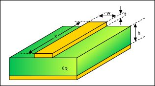
1. Microstrip Line
- Structure: A fixed-width metal trace on an outer layer, with a solid ground plane on the immediately adjacent lower layer.
- Impedance Determinants: Trace width, dielectric layer thickness, and dielectric material type.
- Standard Impedance: Typically 50Ω or 75Ω for RF applications.
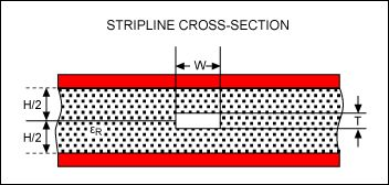
2. Stripline
- Structure: A fixed-width trace on an inner layer, sandwiched between upper and lower ground planes.
- Variants:
- Centered stripline (conductor midway between ground planes)
- Offset stripline (for PCBs with unequal layer thicknesses)
- Application: Ideal for routing RF traces on inner layers.
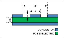
3. Grounded Coplanar Waveguide (CPW-G)
- Structure: A central conductor with ground regions on both sides and a ground plane below.
- Key Advantage: Provides superior isolation between adjacent RF lines and other signal lines.
- Critical Design Rule: Install via fences along both sides of the central conductor. These ground vias short-circuit loop currents induced on the top layer to the underlying ground plane.
Important Notes for Characteristic Impedance Calculation
- Use Specialized Calculation Tools: Dedicated impedance calculators are recommended to determine the correct signal conductor width for the target impedance.
- Dielectric Constant (εR) Variation:
- FR-4 inner core layers: εR ≈ 4.2
- FR-4 outer prepreg layers: εR ≈ 3.8 (lower due to lower glass fiber content)
- Standard Copper Thickness: Calculations are typically based on 1oz copper (1.4 mils / 0.036mm) unless otherwise specified.
About Maxipcb
Maxipcb empowers innovators to turn cutting-edge technologies into reality.
We offer one-stop solutions for design, simulation, testing, PCB manufacturing, component procurement and SMT assembly, enabling efficient development, rapid deployment and risk control across the full product lifecycle.Serving the world in communications, industrial automation, aerospace, automotive, semiconductor and beyond, we build a safer, more connected future together.